
Datasheet


Detailed Description
RESET and RESET Outputs
The MAX691A/MAX693A/MAX800L/MAX800M’s
RESET
and RESET outputs ensure that the μP (with reset inputs
asserted either high or low) powers up in a known state,
and prevents code-execution errors during power-down
or brownout conditions.
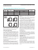
The RESET output is active low, and typically sinks 3.2mA
at 0.1V saturation voltage in its active state. When deas-
serted, RESET sources 1.6mA at typically V
OUT
- 0.5V.
RESET output is open drain, active high, and typically
sinks 3.2mA with a saturation voltage of 0.1V. When no
backup battery is used, RESET output is guaranteed to be
valid down to V
CC
= 1V, and an external 10kΩ pulldown
resistor on RESET insures that it will be valid with V
CC
down to GND (Figure 1). As V
CC
goes below 1V, the gate
drive to the RESET output switch reduces accordingly,
increasing the R
DS(ON)
and the saturation voltage. The
10kΩ pulldown resistor insures the parallel combination
of switch plus resistor is around 10kΩ and the output
saturation voltage is below 0.4V while sinking 40μA. When
using a 10kΩ external pulldown resistor, the high state for
RESET output with V
CC
= 4.75V will be 4.5V typical.
PIN
NAME
FUNCTION
1
VBATT
Battery-Backup
Input. Connect to external battery or
capacitor
and
charging
circuit. If backup battery is
not
used, connect to GND.
2
V
OUT
Output Supply Voltage. When V
CC
is greater than VBATT and above the reset threshold, V
OUT
connects
to
V
CC
. When V
CC
falls below VBATT and is below the reset threshold, V
OUT
connects to VBATT. Connect
a
0.1µF
capacitor from V
OUT
to GND. Connect V
OUT
to V
CC
if no backup battery is
used.
3
V
CC
Input Supply Voltage, 5V
Input.
4
GND Ground. 0V reference for all
signals.
5
BATT
ON
Battery-On Output.
When
V
OUT
switches to
VBATT, BATT
ON goes high.
When
V
OUT
switches to V
CC,
BATT
ON goes low. Connect the base of a PNP through a
current-limiting
resistor to BATT ON for V
OUT
current
require-
ments greater than
250mA.
6
LOW LINE
LOW LINE output goes low when V
CC
falls below the reset threshold. It returns high as soon as V
CC
rises above
the reset threshold.
7
OSC
IN
External
Oscillator Input. When OSC
SEL
is unconnected or driven high, a 10µA pull-up connects from V
OUT
to
OSC IN, the internal oscillator sets the reset and
watchdog
timeout periods, and OSC IN selects between
fast
and slow watchdog timeout periods. When OSC
SEL
is driven low, the reset and watchdog timeout periods
may be set either by a
capacitor
from OSC IN to ground or by an external clock at OSC IN (Figure
3).
8
OSC SEL
Oscillator Select. When OSC SEL is
unconnected
or driven high, the internal oscillator sets the reset
delay
and
watchdog timeout period. When OSC
SEL
is low, the external oscillator input (OSC IN) is enabled
(Table 1). OSC SEL has a 10µA internal
pull-up.
9
PFI
Power-Fail Input. This is the noninverting input to the power-fail
comparator.
When PFI is less than 1.25V,
PFO goes low. When PFI is not used, connect PFI to GND or V
OUT
.
10
PFO
Power-Fail
Output. This is the output of the power-fail comparator.
PFO
goes low when
PFI
is less than 1.25V.
This is an uncommitted comparator, and has no effect on any other internal
circuitry.
11
WDI
Watchdog Input. WDI is a three-level input. If WDI remains either high or low for longer than the
watchdog
time-
out period, WDO goes low and reset is asserted for the reset timeout period. WDO remains low until
the next
tran-
sition at WDI. Leaving WDI unconnected disables the watchdog function. WDI connects to an
internal voltage divider between V
OUT
and GND, which sets it to
mid-supply
when left
unconnected.
12 CE
OUT
Chip-Enable Output. CE OUT goes low only when CE IN is low and V
CC
is above the reset threshold. If CE
IN
is
low when reset is asserted, CE OUT will stay low for 15µs or until CE IN goes high, whichever occurs rst.
13 CE
IN
Chip-Enable Input. The input to
chip-enable
gating circuit. If CE IN is not used, connect CE IN to GND or
V
OUT.
14
WDO
Watchdog Output. If WDI remains high or low longer than the watchdog timeout period, WDO goes low and reset
is asserted for the reset timeout period. WDO returns high on the next transition at WDI. WDO remains high
if
WDI
is
unconnected.
15 RESET
RESET Output goes low whenever V
CC
falls below the reset threshold.
RESET
will remain low typically
for
200ms after V
CC
crosses the reset threshold on
power-up.
16 RESET
RESET
is an
active-high
output. It is open drain, and the inverse of RESET.
MAX691A/MAX693A/
MAX800L/MAX800M
Microprocessor Supervisory Circuits
www.maximintegrated.com
Maxim Integrated
│
7
Pin Description