
Datasheet


Monitor Input (IN)
Connect the center point of a resistive divider to IN to
monitor external voltages (see R1 and R2 of the Typical
Operating Circuit). IN has a rising threshold of V
TH
=
0.5V and a falling threshold of 0.495V (5mV hysteresis).
When V
IN
rises above V
TH
and ENABLE is high (or
ENABLE is low) OUT goes high (OUT goes low) after
the programmed t
DELAY
period. When V
IN
falls below
0.495V, OUT goes low (OUT goes high) after a 16µs
delay. IN has a maximum input current of 15nA so
large-value resistors are permitted without adding sig-
nificant error to the resistive divider.
Adjustable Delay (CDELAY)
When V
IN
rises above V
TH
with ENABLE high (ENABLE
low), the internal 250nA current source begins charging
an external capacitor connected from CDELAY to GND.
When the voltage at CDELAY reaches 1V, the output
asserts (OUT goes high or OUT goes low). When the
output asserts, C
CDELAY
is immediately discharged.
Adjust the delay (t
DELAY
) from when V
IN
rises above
V
TH
(with ENABLE high or ENABLE low) to OUT going
high (OUT going low) according to the equation:
t
DELAY
= C
CDELAY
x 4.0 x 10
6
+ 40µs
where C
CDELAY
is the external capacitor from CDELAY
to GND.
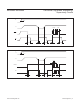
For adjustable delay devices (A version), when V
IN
>
0.5V and ENABLE goes from low to high (ENABLE
goes from high to low) the output asserts after a t
DELAY
period. For nonadjustable delay devices (P version)
there is a 1µs propagation delay from when the enable
input is asserted to when the output asserts. Figures 2
through 5 show the timing diagrams for the adjustable and
fixed delay versions, respectively.
Figure 2. MAX6895A/MAX6897A Timing Diagram
V
CC
V
UVLO
V
TH
V
TH
t
PROPA
t
DL
t
OFF
t
DELAY
t < t
PROPA
t
PROPA
IN
ENABLE
OUT
t > t
PW
www.maximintegrated.com
Maxim Integrated
│
7
MAX6895–MAX6899 Ultra-Small, Adjustable Sequencing/
Supervisory Circuits