
Datasheet


MAX6791–MAX6796
High-Voltage, Micropower, Single/Dual Linear
Regulators with Supervisory Functions
6 _______________________________________________________________________________________
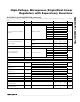
ELECTRICAL CHARACTERISTICS (continued)
(V
IN
= 14V, C
IN
= 1µF, C
OUT
= 10µF, T
A
= T
J
= -40°C to +125°C, unless otherwise noted. Typical values are at T
A
= T
J
= +25°C.)
(Note 1)
PARAMETER SYMBOL CONDITIONS MIN TYP MAX UNITS
LOGIC INPUT (WDS0, WDS1, WD-DIS, WDI)
Input-Voltage Low V
IL
0.4 V
Input-Voltage High V
IH
1.4 V
Input Current Inputs connected to OUT/OUT1 or GND -100 +100 nA
POWER-FAIL COMPARATOR
PFI Threshold V
PFI
1.199 1.231 1.263 V
PFI Hysteresis 0.5 %
PFI Input Current V
PFI
= 14V -100 +100 nA
PFI to PFO Delay (V
PFI
+ 50mV) to (V
PFI
- 50mV) 35 µs
LOGIC OUTPUT (RESET, PFO)
I
SINK
= 50µA (output asserted) 0.3
Output-Voltage Low (Open Drain
or Push-Pull)
V
OL
I
SINK
= 3.2mA (output asserted) 0.4
V
V
OUT
1.0V, I
SOURCE
= 10µA (output not
asserted)
0.8 x
V
OUT
V
OUT
1.5V, I
SOURCE
= 100µA (output not
asserted)
0.8 x
V
OUT
Output-Voltage High (Push-Pull) V
OH
V
OUT
2.2V, I
SOURCE
= 500µA (output not
asserted)
0.8 x
V
OUT
V
Open-Drain Leakage V
RESET
= V
PFO
= 12V (output not asserted) 100 nA
Note 1: All devices are 100% production tested at T
J
= +25°C and +125°C. Limits at -40°C are guaranteed by design.
Note 2: Dropout voltage is defined as (V
IN
- V
OUT
) when V
OUT
is 98% of V
OUT
for V
IN
= 8V.
Note 3: Dropout voltage is defined as (V
IN
- V
OUT
) when V
OUT
is 98% of V
OUT
for V
IN
= 6V.
Note 4: Operation beyond the absolute maximum power dissipation is not guaranteed and may damage the part.
Note 5: Test at V
IN
= 8V (L/M), V
IN
= 6V (T/S), V
IN
= 5V (Z/Y/W/V).