
Datasheet


MAX6709/MAX6714
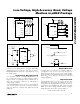
Low-Voltage, High-Accuracy, Quad Voltage
Monitors in µMAX Package
2 _______________________________________________________________________________________
ABSOLUTE MAXIMUM RATINGS
ELECTRICAL CHARACTERISTICS (MAX6709)
(V
CC
= 2.0V to 5.5V, T
A
= -40°C to +85°C, unless otherwise noted. Typical values are at V
CC
= 5V and T
A
= +25°C.) (Note 1)
Stresses beyond those listed under “Absolute Maximum Ratings” may cause permanent damage to the device. These are stress ratings only, and functional
operation of the device at these or any other conditions beyond those indicated in the operational sections of the specifications is not implied. Exposure to
absolute maximum rating conditions for extended periods may affect device reliability.
All Pins to GND.........................................................-0.3V to +6V
Input/Output Current (all pins) ............................................20mA
Continuous Power Dissipation (T
A
= +70°C)
10-Pin µMAX (derate 5.6mW/°C above +70°C) ..........444mW
Operating Temperature Range ...........................-40°C to +85°C
Storage Temperature Range .............................-65°C to +150°C
Junction Temperature......................................................+150°C
Lead Temperature (soldering, 10s) .................................+300°C
PARAMETER
SYMBOL
CONDITIONS
MIN
TYP
MAX
UNITS
Supply Voltage Range V
CC
2.0 5.5 V
V
CC
= 3V 25 50
Supply Current I
CC
V
CC
= 5V 35 65
µA
V
IN_
= input threshold voltage 25 40
Input Current I
IN_
V
IN_
= 0 to 0.85V (for adjustable threshold) 0.2
µA
5.0V (-5%)
4.50 4.63 4.75
5.0V (-10%)
4.25 4.38 4.50
3.3V (-5%)
3.00 3.08 3.15
3.3V (-10%)
2.85 2.93 3.00
3.0V (-5%)
2.70 2.78 2.85
3.0V (-10%)
2.55 2.63 2.70
2.5V (-5%)
2.25 2.32 2.38
2.5V (-10%)
2.13 2.19 2.25
1.8V (-5%)
1.62 1.67 1.71
Threshold Voltage V
TH
IN_ decreasing
1.8V (-10%)
1.53 1.58 1.62
V
Adjustable Threshold V
TH
IN_ decreasing
0.609 0.623 0.635
V
Threshold Voltage Temperature
Coefficient
TCV
TH
60
ppm/°C
Threshold Hysteresis V
HYST
0.3 x V
TH
%
V
IN
_ falling at 10mV/µs from
V
TH
to (V
TH
- 50mV)
30
Propagation Delay
t
PD
V
IN
_ rising at 10mV/µs from
V
TH
to (V
TH
+ 50mV)
5
µs
V
CC
= 5V, I
SINK
= 2mA 0.3
V
CC
= 2.5V, I
SINK
= 1.2mA 0.3
Output Low Voltage V
OL
V
CC
= 1V, I
SINK
= 50µA (Note 2) 0.3
V
Output High Voltage V
OH
V
CC
≥ 2.0V, I
SOURCE
= 6µA (min), PWRGD_
unasserted
0.8 x V
CC
V
Output High Source Current I
OH
V
CC
≥ 2.0V, PWRGD_ unasserted
10 µA