
Datasheet


MAX6457–MAX6460
High-Voltage, Low-Current Voltage Monitors in
SOT Packages
8
Maxim Integrated
Detailed Description
Each of the MAX6457–MAX6460 high-voltage (4V to
28V), low-power voltage monitors include a precision
bandgap reference, one or two low-offset-voltage com-
parators, internal threshold hysteresis, internal timeout
period, and one or two high-voltage open-drain outputs.
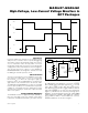
Programming the Trip Voltage (V
TRIP
)
Two external resistors set the trip voltage, V
TRIP
(Figure 5).
V
TRIP
is the point at which the applied voltage (typically
V
CC
) toggles OUT. The MAX6457/MAX6458/MAX6459/
MAX6460’s high input impedance allows large-value
resistors without compromising trip-voltage accuracy.
To minimize current consumption, select a value for R2
between 10kΩ and 1MΩ, then calculate R1 as follows:
where V
TRIP
= desired trip voltage (in volts), V
TH
=
threshold trip voltage (V
TH
+ for overvoltage detection
or V
TH
- for undervoltage detection).
Use the MAX6460 voltage reference (REF) to set the
trip threshold by connecting IN+ or IN- through a volt-
age divider (within the inputs common-mode voltage
range) to REF. Do not connect REF directly to IN+ or
IN- since this violates the input common-mode voltage
range. Small leakage currents into the comparators
inputs allows use of large value resistors to prevent
loading the reference and affecting its accuracy. Figure
5b shows an active-high power-good output. Use the
following equation to determine the resistor values
when connecting REF to IN-:
where V
REF
= reference output voltage (2.25V, typ),
V
REFD
= divided reference, V
TRIP
= desired trip thresh-
old in (in volts).
For an active-low power-good output, connect the
resistor divider R1 and R2 to the inverting input and the
reference-divider network to the noninverting input.
Alternatively, connect an external reference less than
1.4V to either input.
RR
V
V
TRIP
REFD
12 1=−
⎛
⎝
⎜
⎞
⎠
⎟
VV
R
RR
REFD REF
=
+
⎛
⎝
⎜
⎞
⎠
⎟
4
34
RR
V
V
TRIP
TH
12 1=
⎛
⎝
⎜
⎞
⎠
⎟
-
V
CC
IN+
GND
OUT
(OUTA FOR
MAX6459)
R1
V
CC
R2
R
PULLUP
OUT
(OUTA)
MAX6457–
MAX6460
V
TRIP
= V
TH
R1 + R2
R2
Figure 5a. Programming the Trip Voltage
V
CC
IN+
REF
IN-
GND
R1
V
TRIP
V
REFD
R2
R3
R4
R
PULLUP
OUTOUT
MAX6460
Figure 5b. Programming the MAX6460 Trip Voltage
V
TH+
V
TH-
V
IN+
V
OUT
0
V
CC
V
HYST
t
TP
t
TP
Figure 6. Input and Output Waveforms (Noninverting Input Varied)