
Datasheet


MAX6365–MAX6368
SOT23, Low-Power µP Supervisory Circuits
with Battery Backup and Chip-Enable Gating
4 _______________________________________________________________________________________
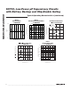
Typical Operating Characteristics
(T
A
= +25°C, unless otherwise noted.)
8
10
9
12
11
15
14
13
16
-40 0-20 20 40 60 80
SUPPLY CURRENT
vs. TEMPERATURE (NO LOAD)
MAX6365/8-01
TEMPERATURE (°C)
SUPPLY CURRENT (µA)
V
CC
= 5.0V
V
BATT
= 0V
0
0.2
0.6
0.4
0.8
1.0
1.2
BATTERY SUPPLY CURRENT
(BACKUP MODE) vs. TEMPERATURE
MAX6365/8-02
TEMPERATURE (°C)
BATTERY SUPPLY CURRENT (µA)
-40 20 40-20 0 60 80
V
BATT
= 2.0V
V
CC
= 0
V
BATT
= 2.8V
0
2
1
4
3
7
6
5
8
-40 0-20 20 40 60 80
BATT-TO-OUT ON-RESISTANCE
vs. TEMPERATURE
MAX6365/8-03
TEMPERATURE (°C)
BATT-TO-OUT ON-RESISTANCE (Ω)
V
BATT
= 5.0V
V
BATT
= 2.0V
V
BATT
= 2.8V
I
OUT
= 25mA
V
CC
= 0V
ELECTRICAL CHARACTERISTICS (continued)
(V
CC
= +2.4V to +5.5V, V
BATT
= +3.0V, CE IN = V
CC
, reset not asserted, T
A
= -40°C to +85°C. Typical values are at T
A
= +25°C,
unless otherwise noted.) (Note 1)
PARAMETER
SYMBOL
CONDITIONS
MIN
TYP
MAX
UNITS
RESET IN (MAX6368 only)
RESET IN Threshold V
RTH
1.185 1.235 1.285
V
RESET IN Leakage Current
±0.01 ±25
nA
RESET IN to Reset Delay V
OD
= 50mV, RESET IN falling 1.5 µs
CHIP-ENABLE GATING
CE IN Leakage Current Reset asserted
±1
µA
CE IN to CE OUT Resistance
Reset not asserted (Note 4) 20
100
Ω
CE OUT Short-Circuit Current Reset asserted, V
CE OUT
= 0V
0.75 2.0
mA
V
CC
= 4.75V 1.5 7
CE IN to CE OUT Propagation
Delay
50Ω source,
C
LOAD
= 6365 50pF
V
CC
= 3.15V 2 9
ns
V
CC
= 5V, V
CC
>
V
BATT
, I
SOURCE
= 100µA
0.8
✕
V
CC
CE OUT Output Voltage High
V
CC
= 0V, V
BATT
>
2.2V, I
SOURCE
= 1µA
V
BATT
-
0.1
V
Reset-to-CE OUT Delay 12 µs
Note 1: All devices are 100% production tested at T
A
= +25°C. Limits over temperature are guaranteed by design.
Note 2: V
BATT
can be 0V anytime, or V
CC
can go down to 0V if V
BATT
is active (except at startup).
Note 3: RESET is pulled up to OUT. Specifications apply for OUT = V
CC
or OUT = BATT.
Note 4: The chip-enable resistance is tested with V
CC
= V
TH(MAX)
and V
CE IN
= V
CC
/2.