
Datasheet


MAX6126
Ultra-High-Precision, Ultra-Low-Noise,
Series Voltage Reference
14
Maxim Integrated
Detailed Description
Wideband Noise Reduction
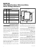
To improve wideband noise and transient power-supply
noise, add a 0.1µF capacitor to NR (Figure 1). Larger
values do not improve noise appreciably. A 0.1µF NR
capacitor reduces the noise from 60nV/√Hz to
35nV/√Hz for the 2.048V output. Noise in the power-
supply input can affect output noise, but can be
reduced by adding an optional bypass capacitor
between IN and GND, as shown in the
Typical
Operating Circuit
.
Output Bypassing
The MAX6126 requires an output capacitor between
0.1µF and 10µF. Locate the output capacitor as close
to OUTF as possible. For applications driving switching
capacitive loads or rapidly changing load currents, it is
advantageous to use a 10µF capacitor in parallel with a
0.1µF capacitor. Larger capacitor values reduce tran-
sients on the reference output.
Supply Current
The quiescent supply current of the series-mode
MAX6126 family is typically 380µA and is virtually inde-
pendent of the supply voltage, with only a 2µA/V (max)
variation with supply voltage.
When the supply voltage is below the minimum speci-
fied input voltage during turn-on, the device can draw
up to 300µA beyond the nominal supply current. The
input voltage source must be capable of providing this
current to ensure reliable turn-on.
Thermal Hysteresis
Thermal hysteresis is the change of output voltage at
T
A
= +25°C before and after the device is cycled over
its entire operating temperature range. The typical ther-
mal hysteresis value is 20ppm (SO package).
Turn-On Time
These devices typically turn on and settle to within
0.1% of their final value in 200µs to 2ms depending on
the device. The turn-on time can increase up to 4ms
with the device operating at the minimum dropout volt-
age and the maximum load. A noise reduction capaci-
tor of 0.1µF increases the turn-on time to 20ms.
Output Force and Sense
The MAX6126 provides independent connections for the
power-circuit output (OUTF) supplying current into a
load, and for the circuit input regulating the voltage
applied to that load (OUTS). This configuration allows for
the cancellation of the voltage drop on the lines connect-
ing the MAX6126 and the load. When using the Kelvin
connection made possible by the independent current
and voltage connections, take the power connection to
the load from OUTF, and bring a line from OUTS to join
the line from OUTF, at the point where the voltage accu-
Pin Description
PIN NAME FUNCTION
1NR
Noise Reduction. Connect a 0.1µF
capacitor to improve wideband noise.
Leave unconnected if not used (see
Figure 1).
2 IN Positive Power-Supply Input
3 GND Ground
4 GNDS
Ground-Sense Connection. Connect to
ground connection at load.
5, 8 I.C.
Internally Connected. Do not connect
anything to these pins.
6 OUTS Voltage Reference Sense Output
7 OUTF
Voltage Reference Force Output. Short
OUTF to OUTS as close to the load as
possible. Bypass OUTF with a
capacitor (0.1µF to 10µF) to GND.
NR
OUTF
*OPTIONAL.
0.1µF*
OUTS
REFERENCE
OUTPUT
(V
OUT
+ 200mV) TO 12.6V INPUT
IN
GND
GNDS
MAX6126
*
Figure 1. Noise-Reduction Capacitor