
Datasheet


MAX5986A–MAX5986C/MAX5987A
IEEE 802.3af-Compliant, High-Efficiency, Class 1/
Class 2, PDs with Integrated DC-DC Converter
17Maxim Integrated
PCB Layout
Careful PCB layout is critical to achieve clean and stable
operation. It is highly recommended to duplicate the
MAX5986A EV kit layout for optimum performance. If
deviation is necessary, follow these guidelines for good
PCB layout:
1) Connect input and output capacitors to the power
ground plane; connect all other capacitors to the sig-
nal ground plane.
2) Place capacitors on V
DD
, V
CC
, AUX, V
DRV
as close
as possible to the IC and its corresponding pin using
direct traces. Keep power ground plane (connected
to PGND) and signal ground plane (connected to
GND) separate.
3) Keep the high-current paths as short and wide as
possible. Keep the path of switching current short
and minimize the loop area formed by LX, the output
capacitors, and the input capacitors.
4) Connect V
DD
, V
CC
, and PGND separately to a large
copper area to help cool the IC to further improve
efficiency and long-term reliability.
5) Ensure all feedback connections are short and direct.
Place the feedback resistors and compensation com-
ponents as close as possible to the IC.
6) Route high-speed switching nodes, such as LX, away
from sensitive analog areas (FB).
7) Place enough vias in the pad for the EP of the
MAX5986A–MAX5986C/MAX5987A so that heat gener-
ated inside can be effectively dissipated by the PCB
copper. The recommended spacing for the vias is 1mm
to 1.2mm pitch. The thermal vias should be plated (1oz
copper) and have a small barrel diameter (0.3mm to
0.33mm).
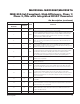
Table 1. Design Selection Table
OUTPUT C
IN
C
OUT
L CLASS
3.3V
CERAMIC ELECTROLYTIC CERAMIC
2.2FF/100V 10FF/63V 3x22FF/6.3V 33FH/1.4A 1
5V 2.2FF/100V 10FF/63V 3x22FF/6.3V 47FH/1.6A 1 or 2
12V 2.2FF/100V 10FF/63V 2x10FF/16V 220F/0.8A* 1 or 2
*100μH/0.8A is recommendedfor with the MAX5986C.