
Datasheet


IEEE 802.3af/at-Compliant, Powered Device Interface
Controllers with Integrated 70W High-Power MOSFET
MAX5982A/MAX5982B/MAX5982C
_______________________________________________________________________________________ 7
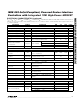
Pin Description
Pin Configurations
PIN
NAME FUNCTION
MAX5982A/
MAX5982B
MAX5982C
1 1, 13–16 N.C. No Connection. Not internally connected.
2 2 V
DD
Positive Supply Input. Connect a 68nF (min) bypass capacitor between V
DD
and V
SS
.
3 3 DET
Detection Resistor Input. Connect a signature resistor (R
DET
= 24.9kI) from DET to V
DD
.
4 4 I.C. Internally Connected. Leave unconnected.
5, 6 5, 6 V
SS
Negative Supply Input. V
SS
connects to the source of the integrated isolation n-channel
power MOSFET.
7, 8 7, 8 RTN
Drain of Isolation MOSFET. RTN connects to the drain of the integrated isolation
n-channel power MOSFET. Connect RTN to the downstream DC-DC converter ground as
shown in the Typical Application Circuit.
9 9 WAD
Wall Power Adapter Detector Input. Wall adapter detection is enabled the moment
V
DD
- V
SS
crosses the mark event threshold. Detection occurs when the voltage from
WAD to RTN is greater than 9V. When a wall power adapter is present, the isolation
n-channel power MOSFET turns off and 2EC current sink turns on. Connect WAD directly
to RTN when the wall power adapter or other auxiliary power source is not used.
10 10 PG
Open-Drain, Power-Good Indicator Output. PG sinks 230FA to disable the downstream
DC-DC converter while turning on the hot-swap MOSFET switch. PG current sink is
disabled during detection, classification, and in the steady-state power mode. The PG
current sink is turned on to disable the downstream DC-DC converter when the device is
in sleep mode.
3
4
2
1
10
9
11
V
SS
RTN
V
SS
*EP
LED
56
V
DD
8
16 15 13
DET
I.C.
CLS
2EC
PG
WAD
MAX5982A
MAX5982B
RTN
7
14
N.C.
TQFN
12
ULP
WK
SL
*CONNECT EP TO V
SS
.
+
TQFN
TOP VIEW
+
3
4
2
1
10
9
11
V
SS
RTN
V
SS
*EP
N.C.
N.C.
N.C.
56
V
DD
8
16 15 13
DET
I.C.
CLS
2EC
PG
WAD
MAX5982C
RTN N.C.
7
14
N.C.
12