
Datasheet


22 Maxim Integrated
Active-Clamped, Spread-Spectrum,
Current-Mode PWM Controllers
MAX5974A/MAX5974B/MAX5974C/MAX5974D
Programmable Slope Compensation
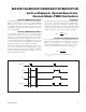
The device generates a current ramp at CSSC such that
its peak is 50FA at 80% duty cycle of the oscillator. An
external resistor connected from CSSC to the CS then
converts this current ramp into programmable slope-
compensation amplitude, which is added to the current-
sense signal for stability of the peak current-mode
control loop. The ramp rate of the slope compensation
signal is given by:
CSSC SW
R 50 A f
m
80%
× µ×
=
where m is the ramp rate of the slope-compensation
signal, R
CSSC
is the value of the resistor connected
between CSSC and CS used to program the ramp rate,
and f
SW
is the switching frequency.
Error Amplifier
The MAX5974A/MAX5974B include an internal error
amplifier with a sample-and-hold input. The feedback
input of the MAX5974C/MAX5974D is continuously con-
nected. The noninverting input of the error amplifier is
connected to the internal reference and feedback is
provided at the inverting input. High open-loop gain and
unity-gain bandwidth allow good closed-loop bandwidth
and transient response. Calculate the power-supply out-
put voltage using the following equation:
FB1 FB2
OUT REF
FB2
RR
VV
R
+
= ×
where V
REF
= 1.52V for the MAX5974A/MAX5974B
and V
REF
= 1.215V for the MAX5974C/MAX5974D. The
amplifier’s noninverting input is internally connected to
a soft-start circuit that gradually increases the reference
voltage during startup. This forces the output voltage to
come up in an orderly and well-defined manner under
all load conditions.
Applications Information
Startup Time Considerations
The bypass capacitor at IN, C
IN
, supplies current
immediately after the devices wake up (see the Typical
Application Circuits). Large values of C
IN
increase
the startup time, but also supply gate charge for more
cycles during initial startup. If the value of C
IN
is too
small, V
IN
drops below 7V because NDRV does not have
enough time to switch and build up sufficient voltage
across the tertiary output (MAX5974C/MAX5974D) or
coupled inductor output (MAX5974A/MAX5974B), which
powers the device. The device goes back into UVLO
and does not start. Use a low-leakage capacitor for C
IN
.
Typically, offline power supplies keep startup times to
less than 500ms even in low-line conditions (85V AC
input for universal offline or 36V DC for telecom applica-
tions). Size the startup resistor, R
IN
, to supply both the
maximum startup bias of the device (150FA) and the
charging current for C
IN
. C
IN
must be charged to 16V
within the desired 500ms time period. C
IN
must store
enough charge to deliver current to the device for at
least the soft-start time (t
SS
) set by C
SS
. To calculate the
approximate amount of capacitance required, use the
following formula:
G GTOT SW
IN G SS
IN
HYST
IQ f
(I I )(t )
C
V
=
+
=
where I
IN
is the ICs’ internal supply current (1.8mA)
after startup, Q
GTOT
is the total gate charge for the
n-channel and p-channel FETs, f
SW
is the ICs’ switch-
ing frequency, V
HYST
is the bootstrap UVLO hysteresis
(9V typ), and t
SS
is the soft-start time. R
IN
is then cal-
culated as follows:
S(MIN) INUVR
IN
START
VV
R
I
−
≅
where V
S(MIN)
is the minimum input supply voltage for
the application (36V for telecom), V
INUVR
is the boot-
strap UVLO wake-up level (16V), and I
START
is the IN
supply current at startup (150FA max).