
Datasheet


MAX5898
16-Bit, 500Msps, Interpolating and Modulating
Dual DAC with Interleaved LVDS Inputs
12 ______________________________________________________________________________________
Detailed Description
The MAX5898 dual, 500Msps, high-speed, 16-bit, cur-
rent-output DAC provides superior performance in com-
munication systems requiring low-distortion analog-signal
reconstruction. The MAX5898 combines two DAC cores
with 8x/4x/2x programmable digital interpolation filters, a
digital quadrature modulator, an SPI-compatible serial
interface for programming the device, and an on-chip
1.2V reference. Individual DAC channel gain and offset
adjustments are available to compensate for downstream
signal-path imbalances. The full-scale output current
range is adjustable from 2mA to 20mA to optimize power
dissipation and gain control.
Each channel contains three selectable interpolating fil-
ters making the MAX5898 capable of 2x, 4x, 8x, or no
interpolation, which allows for low input data rates and
high DAC update rates. When operating in 8x interpola-
tion mode, the interpolator increases the DAC conversion
rate by a factor of eight, providing an eight-fold increase
in separation between the reconstructed waveform spec-
trum and its first image. The MAX5898 accepts either
two’s complement or offset binary input data format on a
single interleaved LVDS input bus.
The MAX5898 includes modulation modes at f
IM
/ 2 and
f
IM
/ 4, where f
IM
is the data rate at the input of the mod-
ulator. If 2x interpolation is used, this data rate is 2x the
input data rate. If 4x or 8x interpolation is used, this data
rate is 4x the input data rate. Table 1 summarizes the
modulator operating data rates.
The power-down modes can be used to turn off each
DAC’s output current or the entire digital section.
Programming both DACs into power-down simultane-
ously powers down the digital interpolation filters. Note
that the SPI section is always active.
The analog and digital sections of the MAX5898 have
separate power-supply inputs (AV
DD3.3
, AV
DD1.8
,
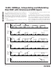
Functional Diagram
IDAC
OUTIP
OUTIN
QDAC
OUTQP
OUTQN
SELIQ
D0–D15
SERIAL INTERFACE
CONTROL REGISTERS
REFERENCE
MODULATOR
CLOCK BUFFERS
AND DIVIDERS
CLKPCLKN
RESET
f
CLK
f
DAC
f
DAC
DATA SYNCH
AND DEMUX
MUX
Q
I
Q
I
2x
INTERPOLATING
FILTER
2x
INTERPOLATING
FILTER
2x
INTERPOLATING
FILTER
2x
INTERPOLATING
FILTER
2x
INTERPOLATING
FILTER
2x
INTERPOLATING
FILTER
MUX
MUX
MUX
MUX
MUX
MUX
MUX
MUX
MUX
DIGITAL
OFFSET
ADJUST
DIGITAL
OFFSET
ADJUST
DIGITAL
GAIN
ADJUST
/2/2
DOUT DIN CS SCLK DACREF FSADJ REFIO
DATACLK
∑
∑
∑
f
IM
/ 2, f
IM
/ 4
∑
DIGITAL
GAIN
ADJUST
/2/2
MAX5898