
Datasheet


MAX5813/MAX5814/MAX5815
Ultra-Small, Quad-Channel, 8-/10-/12-Bit Buffered
Output DACs with Internal Reference and I
2
C Interface
26Maxim Integrated
Applications Information
Power-On Reset (POR)
When power is applied to V
DD
and V
DDIO
, the DAC out-
put is set to zero scale. To optimize DAC linearity, wait
until the supplies have settled and the internal setup and
calibration sequence completes (200Fs, typ).
Power Supplies and
Bypassing Considerations
Bypass V
DD
and V
DDIO
with high-quality ceramic capac-
itors to a low-impedance ground as close as possible to
the device. Minimize lead lengths to reduce lead induc-
tance. Connect the GND to the analog ground plane.
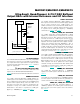
Layout Considerations
Digital and AC transient signals on GND can create noise
at the output. Connect GND to form the star ground for
the DAC system. Refer remote DAC loads to this system
ground for the best possible performance. Use proper
grounding techniques, such as a multilayer board with a
low-inductance ground plane, or star connect all ground
return paths back to the MAX5813/MAX5814/MAX5815
GND. Carefully layout the traces between channels to
reduce AC cross-coupling. Do not use wire-wrapped
boards and sockets. Use shielding to minimize noise immu-
nity. Do not run analog and digital signals parallel to one
another, especially clock signals. Avoid routing digital lines
underneath the MAX5813/MAX5814/MAX5815 package.
Definitions
Integral Nonlinearity (INL)
INL is the deviation of the measured transfer function
from a straight line drawn between two codes once offset
and gain errors have been nullified.
Differential Nonlinearity (DNL)
DNL is the difference between an actual step height and
the ideal value of 1 LSB. If the magnitude of the DNL P
1 LSB, the DAC guarantees no missing codes and is
monotonic. If the magnitude of the DNL R 1 LSB, the DAC
output may still be monotonic.
Offset Error
Offset error indicates how well the actual transfer function
matches the ideal transfer function. The offset error is
calculated from two measurements near zero code and
near maximum code.
Gain Error
Gain error is the difference between the ideal and the
actual full-scale output voltage on the transfer curve,
after nullifying the offset error. This error alters the slope
of the transfer function and corresponds to the same
percentage error in each step.
Zero-Scale Error
Zero-scale error is the difference between the DAC
output voltage when set to code zero and ground. This
includes offset and other die level nonidealities.
Full-Scale Error
Full-scale error is the difference between the DAC output
voltage when set to full scale and the reference voltage.
This includes offset, gain error, and other die level noni-
dealities.
Settling Time
The settling time is the amount of time required from the
start of a transition, until the DAC output settles to the new
output value within the converter’s specified accuracy.
Digital Feedthrough
Digital feedthrough is the amount of noise that appears
on the DAC output when the DAC digital control lines are
toggled.
Digital-to-Analog Glitch Impulse
A major carry transition occurs at the midscale point
where the MSB changes from low to high and all other
bits change from high to low, or where the MSB changes
from high to low and all other bits change from low to
high. The duration of the magnitude of the switching
glitch during a major carry transition is referred to as the
digital-to-analog glitch impulse.
The digital-to-analog power-up glitch is the duration of
the magnitude of the switching glitch that occurs as the
device exits power-down mode.