
Datasheet


MAX5742
12-Bit, Low-Power, Quad, Voltage-Output
DAC with Serial Interface
______________________________________________________________________________________ 11
Applications Information
Unipolar Output
The typical application circuit (Figure 3) shows the
MAX5742 configured for a unipolar output, where the
output voltages and the reference inputs have the
same polarity. Table 3 lists the unipolar output codes.
Bipolar Output
The MAX5742 can be configured for bipolar operation
using a dual supply op amp (Figure 4). The transfer
function for bipolar operation is:
where NB is the decimal value of the DACs binary input
code. Table 4 shows digital codes (offset binary) and
corresponding output voltages for the circuit in Figure 4.
Power Supply and Layout Considerations
Careful PC board layout is important for optimal system
performance. To reduce noise injection and digital feed-
through, keep analog and digital signals separate.
Ensure that that the return path from GND to the supply
ground is short and low impedance. Use a ground
plane. Bypass V
DD
to GND with a 0.1µF capacitor as
close as possible to V
DD
.
VV
2NB
4096
OUT REF
=
−
1
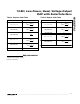
CONTENTS OF SHIFT REGISTER
D15 (MSB) D0 (LSB)
C3 C2 C1 C0 D11 D10 D9 D8 D7 D6 D5 D4 D3 D2 D1 D0
Figure 1. 16-Bit Input Word
SCLK X 1 2 3
t
CL
t
OS
t
CSPWH
t
CSS
t
CSH
t
OH
t
CH
456 16X
X C3 C2 C1 C0 D11 D10 D0D1 XDIN
CS
Figure 2. Timing Diagram