
Datasheet


MAX5732–MAX5735
32-Channel, 16-Bit, Voltage-Output
DACs with Serial Interface
18 ______________________________________________________________________________________
C2, C1, and C0 = 010, address bits A5–A0 = 111111,
and all data bits to don’t care. See Table 3 for the data
format. This operation updates all DAC outputs.
Note: The software load DAC does not affect the offset DAC.
Clear (
CLR
)
The MAX5732–MAX5735 feature an active-low CLR
logic input that sets all channels including the offset
DAC to 0V (code 0000hex). The offset DAC needs to be
reprogrammed after CLR is asserted. Driving CLR low
clears the contents of both the input and DAC registers.
The serial interface can also issue a software clear com-
mand. Setting the control bits C2, C1, and C0 = 111
(Table 4) performs the same function as driving logic-
input CLR low. Table 4 shows the clear-data format for
the software-controlled clear command. This register-
reset process cannot be interrupted. All serial input data
is ignored until the entire reset process is complete.
Serial Interface
A 3-wire SPI-/QSPI-/MICROWIRE- and DSP-compatible
serial interface controls the MAX5732–MAX5735. The
interface requires a 32-bit command word to control the
device. The command word consists of 3 control bits, 6
address bits, 7 don’t-care bits, and 16 data bits. Table 5
shows the general serial-data format. The control bits
control various write and read commands as well as the
load DAC and clear commands. Table 6 shows the con-
trol-bit functions. The address bits select the register(s)
to be written. Table 7 shows the address functions. The
data bits control the value of the DAC outputs.
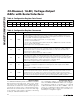
Table 3. Load-DAC Data Format
CONTROL
BITS
ADDRESS
BITS
DON’T-
CARE
BITS
DATA BITS
C2, C1,
AND C0
A5–A0 — D15–D0
010 111111 XXXXXXX XXXXXXXXXXXXXXXX
Table 4. Clear-Data Format
CONTROL
BITS
ADDRESS
BITS
DON’T-
CARE
BITS
DATA BITS
C2, C1,
AND C0
A5–A0 — D15–D0
111 See table 7 XXXXXXX XXXXXXXXXXXXXXXX
Table 5. Serial-Data Format
CONTROL
BITS
ADDRESS
BITS
DON’T-
CARE
BITS
DATA BITS
MSB LSB
C2, C1,
and C0
A5–A0 XXXXXXX D15–D0
Table 6. Control-Bit Functions
CONTROL
BITS
C2 C1 C0
CONTROL-BIT DESCRIPTION
000
No operation (NOP); no internal registers
change state. The NOP command can be
passed to DOUT depending on the state of the
configuration register. Address bits A5–A0 and
data bits D15–D0 are ignored.
001
Loads D15–D0 into the input register(s) for the
selected address. Depending on the address
bits, this command could write to:
The configuration register (A[5:0] = 100001)
One of the i np ut r eg i ster s of the 32 D AC channel s
All 32 DAC input registers (A[5:0] = 111111)
The offset D AC i np ut r eg i ster ( A[ 5:0] = 100000)
010
Loads DAC register(s) from the input register(s).
Depending on the address bits, this command
can update one or all of the DAC registers from
the stored input register value(s). Data bits
D15–D0 are ignored.
011
Write-through; loads D15–D0 into the input and
DAC registers, depending on the address bits.
100
Read command; depending on the address bits,
one of the DAC-register values or the
configuration-register value may be read back
through DOUT. Data bits D15–D0 are ignored.
1 0 1 Reserved for internal testing; do not use.
1 1 0 Reserved for internal testing; do not use.
111
C l ear r eg i ster ( s) ; d ep end i ng on the ad d r ess b i ts,
one or al l r eg i ster s ( excep t the offset- D AC r eg i ster s)
ar e cl ear ed to zer o. D ata b i ts D 15–D 0 ar e i g nor ed .