
Datasheet


MAX548A/MAX549A/MAX550A
+2.5V to +5.5V, Low-Power, Single/Dual,
8-Bit Voltage-Output DACs in µMAX Package
2 _______________________________________________________________________________________
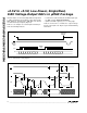
ABSOLUTE MAXIMUM RATINGS
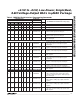
ELECTRICAL CHARACTERISTICS
(V
DD
= +2.5V to +5.5V, T
A
= T
MIN
to T
MAX
, unless otherwise noted. Typical values are at T
A
= +25°C.)
Stresses beyond those listed under “Absolute Maximum Ratings” may cause permanent damage to the device. These are stress ratings only, and functional
operation of the device at these or any other conditions beyond those indicated in the operational sections of the specifications is not implied. Exposure to
absolute maximum rating conditions for extended periods may affect device reliability.
V
DD
, SCLK, DIN, CS, LDAC, OUT_ to GND ...............-0.3V to 6V
REF to GND................................................-0.3V to (V
DD
+ 0.3V)
Maximum Current (any pin) .............................................±50mA
Continuous Power Dissipation (T
A
= +70°C)
Plastic DIP (derate 9.09mW/°C above +70°C) .............727mW
µMAX (derate 4.10mW/°C above +70°C) .....................330mW
Operating Temperature Ranges
MAX5_ _AC_ A.....................................................0°C to +70°C
MAX5_ _AE_ A..................................................-40°C to +85°C
Storage Temperature Range.............................-65°C to +150°C
Lead Temperature (soldering, 10sec).............................+300°C
MAX549A
MAX549A/MAX550A for specified
performance
Guaranteed
monotonic
CONDITIONS
16.7
V2.5 V
DD
V
REF
Reference Input
Voltage Range
±0.9
Bits8NResolution
LSB
±0.9
DNLDifferential Nonlinearity
LSB±1ZCEZero-Code Error
LSB±1FSEFull-Scale Error
UNITSMIN TYP MAXSYMBOLPARAMETER
MAX5_ _AEUA (Note 1)
All others
MAX549A/MAX550A
MAX548A
MAX550A
kΩ33.3R
OUT
DAC Output Resistance
V
0 V
REF
DAC Output Voltage Swing
0 V
DD
kΩ
33.3
R
REF
Reference Input Resistance
DAC Code = 55 Hex (Note 2)
MAX548A/MAX549A %±0.2
∆R
OUT
/
R
OUT
DAC Output Resistance
Matching
±1MAX5_ _AEUA (Note 1)
All others
LSB
±1
TUETotal Unadjusted Error
MAX549A
330 550
150 250
MAX550A
165 275
µA
75 125
I
REF
Reference Input Current
DAC Code = 55 Hex (Note 3)
V
DD
= V
REF
= 5.5V
V
DD
= V
REF
= 2.5V
V
DD
= V
REF
= 5.5V
V
DD
= V
REF
= 2.5V
V0.7V
DD
V
IH
Input High Voltage
V0.3V
DD
V
IL
Input Low Voltage
V
IN
= 0V or V
DD
µA±1I
IN
Input Current
pF10C
IN
Input Capacitance (Note 4)
STATIC PERFORMANCE
REFERENCE INPUT
DAC OUTPUT
DIGITAL INPUTS