
Datasheet


10-Bit, Nonvolatile, Linear-Taper Digital
Potentiometers
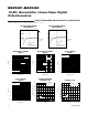
Pin Description
PIN
TQFN TSSOP
NAME FUNCTION
1 12 H High Terminal
2 11 W Wiper Terminal
3 10 L Low Terminal
4–7, 15 7, 8, 9, 13 N.C. No Connection. Not internally connected.
8, 16 14 V
SS
Negative Power-Supply Input. For single-supply operation, connect V
SS
to GND. For dual-
supply operation, -2.5V ≤ V
SS
≤ -0.2V as long as (V
DD
- V
SS
) ≤ +5.25V. Bypass V
SS
to GND
with a 0.1µF ceramic capacitor as close to the device as possible.
9 6 SPI/UD
Interface-Mode Select. Select serial SPI interface when SPI/UD = 1. Select serial up/down
interface when SPI/UD = 0.
Serial SPI Interface Data Input (SPI/UD = 1)
10 5 DIN(U/D)
Up/Down Control Input (SPI/UD = 0). With DIN(U/D) low, a high-to-low SCLK(INC) transition
decrements the wiper position. With DIN(U/D) high, a high-to-low SCLK(INC) transition
increments the wiper position.
Serial SPI Interface Clock Input (SPI/UD = 1)
11 4 SCLK(INC)
Wiper-Increment Control Input (SPI/UD = 0). With CS low, the wiper position moves in the
direction determined by the state of DIN(U/D) on a high-to-low transition.
12 3 CS Active-Low Digital Input Chip Select
13 2 GND Ground
14 1 V
DD
Positive Power-Supply Input (+2.7V ≤ V
DD
≤ +5.25V). Bypass V
DD
to GND with a 0.1µF
ceramic capacitor as close to the device as possible.
— — EP Exposed Pad (TQFN Only). Externally connect EP to V
SS
or leave unconnected.
(MAX5481/MAX5482 Voltage-Dividers)
MAX5481–MAX5484
9
Maxim Integrated