
Datasheet


MAX541/MAX542
+5V, Serial-Input, Voltage-Output, 16-Bit DACs
_______________________________________________________________________________________ 7
Detailed Description
The MAX541/MAX542 voltage-output, 16-bit digital-to-
analog converters (DACs) offer full 16-bit performance
with less than 1LSB integral linearity error and less than
1LSB differential linearity error, thus ensuring monoton-
ic performance. Serial data transfer minimizes the num-
ber of package pins required.
The MAX541/MAX542 are composed of two matched
DAC sections, with a 12-bit inverted R-2R DAC forming
the 12 LSBs and the 4 MSBs derived from 15 identically
matched resistors. This architecture allows the lowest
glitch energy to be transferred to the DAC output on
major-carry transitions. It also lowers the DAC output
impedance by a factor of eight compared to a standard
R-2R ladder, allowing unbuffered operation in medium-
load applications.
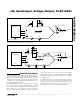
The MAX542 provides matched bipolar offset resistors,
which connect to an external op amp for bipolar output
swings (Figure 2b). For optimum performance, the
MAX542 also provides a set of Kelvin connections to
the voltage-reference and analog-ground inputs.
MAX542
MAX400
AGNDFDGND
(GND)
V
DD
REFF
REFS
R
INV
R
FB
RFB
INV
OUT
LDAC
SCLK
DIN
CS
AGNDS
0.1µF
+5V
EXTERNAL OP AMP
MC68XXXX
PCS0
MOSI
SCLK
IC1
BIPOLAR
OUT
+5V
-5V
0.1µF
+2.5V
10µF
Figure 2b. Typical Operating Circuit—Bipolar Output
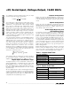
MAX541/MAX542
MAX495
DGND
( ) ARE FOR MAX542 ONLY
(GND)
V
DD
(REFS)REF (REFF)
OUT
SCLK
DIN
CS
AGND_
0.1µF
0.1µF
+5V
+2.5V
EXTERNAL OP AMP
MC68XXXX
PCS0
MOSI
SCLK
UNIPOLAR
OUT
(LDAC)
10µF
Figure 2a. Typical Operating Circuit—Unipolar Output