
Datasheet


Note 2: Guaranteed by design.
Note 3: Crosstalk is defined as the glitch energy at any DAC output in response to a full-scale step change on any other DAC
.
Note 4: Digital inputs at 2.4V; with digital inputs at CMOS levels, I
DD
decreases slightly.
Note 5: All input signals are specified with t
R
= t
F
≤ 5ns. Logic input swing is 0 to 5V.
Note 6: Serial data clocked out of SDO on SCK’s falling edge. (SDO is an open-drain output for the MAX536. The MAX537’s SDO
pin has an internal active pullup.)
Note 7: Serial data clocked out of SDO on SCK’s rising edge.
Note 10: When disabled, SDO is internally pulled high.
MAX536/MAX537
Calibrated, Quad, 12-Bit
Voltage-Output DACs with Serial Interface
_______________________________________________________________________________________ 7
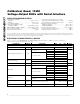
ELECTRICAL CHARACTERISTICS—MAX537 (continued)
(V
DD
= +5V, V
SS
= -5V, REFAB/REFCD = 2.5V, AGND = DGND = 0V, R
L
= 5kΩ, C
L
= 100pF, T
A
= T
MIN
to T
MAX
, unless
otherwise noted. Typical values are at T
A
= +25°C.)
PARAMETER
SYMBOL
CONDITIONS
MIN
TYP
MAX
UNITS
CS Fall to SDO Enable
t
DV
C
LOAD
= 50pF, MAX537_C/E 75 140
ns
CS Rise to DSO Disable (Note 10)
t
TR
C
LOAD
= 50pF, MAX537_C/E 70 130 ns
SCK Rise to CS Fall Delay
t
CSO
Continuous SCK, SCK edge ignored 35
ns
CS Rise to SCK Rise Hold Time
t
CS1
SCK edge ignored, MAX537_C/E 35
ns
LDAC Pulse Width High
t
LDAC
MAX537_C/E 50
ns
CS Pulse Width High
t
CSW
MAX537_C/E 100
ns