
Datasheet


MAX5354/MAX5355
10-Bit Voltage-Output DACs
in 8-Pin µMAX
_______________________________________________________________________________________ 5
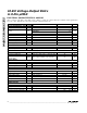
ELECTRICAL CHARACTERISTICS: MAX5355 (continued)
(V
DD
= +3.15V to +3.6V, REF = 1.25V, GND = 0V, R
L
= 5kΩ, C
L
= 100pF, T
A
= T
MIN
to T
MAX
, unless otherwise noted. Typical values
are at T
A
= +25°C. Output buffer connected in unity-gain configuration (Figure 8).)
ns
CONDITIONS
40t
CH
SCLK Pulse Width High
ns100t
CP
SCLK Clock Period
ns40t
CSS
CS Fall to SCLK Rise Setup Time
ns40t
DS
DIN Setup Time
ns0t
CSH
SCLK Rise to CS Rise Hold Time
ns40t
CL
SCLK Pulse Width Low
UNITSMIN TYP MAXSYMBOLPARAMETER
ns40t
CS1
CS Rise to SCLK Rise Hold Time
ns0t
DH
DIN Hold Time
ns100t
CSW
CS Pulse Width High
ns40t
CS0
SCLK Rise to CS Fall Delay
Note 4: Guaranteed from code 6 to code 1023 in unity-gain configuration.
Note 5: Accuracy is better than 1LSB for V
OUT
= 8mV to V
DD
- 150mV, guaranteed by a power-supply rejection test at the
end points.
Note 6: R
L
= ∞, digital inputs at GND or V
DD
.
TIMING CHARACTERISTICS (Figure 6)