
Datasheet


MAX531/MAX538/MAX539
+5V, Low-Power, Voltage-Output
Serial 12-Bit DACs
2 _______________________________________________________________________________________
ABSOLUTE MAXIMUM RATINGS
V
DD
to DGND and V
DD
to AGND................................-0.3V, +6V
V
SS
to DGND and V
SS
to AGND .................................-6V, +0.3V
V
DD
to V
SS
.................................................................-0.3V, +12V
AGND to DGND........................................................-0.3V, +0.3V
Digital Input Voltage to DGND ......................-0.3V, (V
DD
+ 0.3V)
REFIN..................................................(V
SS
- 0.3V), (V
DD
+ 0.3V)
REFOUT to AGND.........................................-0.3V, (V
DD
+ 0.3V)
RFB .....................................................(V
SS
- 0.3V), (V
DD
+ 0.3V)
BIPOFF................................................(V
SS
- 0.3V), (V
DD
+ 0.3V)
V
OUT
(Note 1) ................................................................V
SS
, V
DD
Continuous Current, Any Pin................................-20mA, +20mA
Continuous Power Dissipation (T
A
= +70°C)
8-Pin Plastic DIP (derate 9.09mW/°C above +70°C)....727mW
8-Pin SO (derate 5.88mW/°C above +70°C)................471mW
14-Pin Plastic DIP (derate 10.00mW/°C above +70°C)...800mW
14-Pin SO (derate 8.33mW/°C above +70°C)..............667mW
Operating Temperature Ranges
MAX53_ _C_ _.....................................................0°C to +70°C
MAX53_ _E_ _ ..................................................-40°C to +85°C
Storage Temperature Range.............................-65°C to +165°C
Lead Temperature (soldering, 10sec).............................+300°C
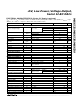
ELECTRICAL CHARACTERISTICS—Single +5V Supply
(V
DD
= +5V ±10%, V
SS
= 0V, AGND = DGND = 0V, REFIN = 2.048V (external), RFB = BIPOFF = VOUT (MAX531), C
REFOUT
= 33µF
(MAX531), R
L
= 10kΩ, C
L
= 100pF, T
A
= T
MIN
to T
MAX
, unless otherwise noted.)
Stresses beyond those listed under “Absolute Maximum Ratings” may cause permanent damage to the device. These are stress ratings only, and functional
operation of the device at these or any other conditions beyond those indicated in the operational sections of the specifications is not implied. Exposure to
absolute maximum rating conditions for extended periods may affect device reliability.
PARAMETER SYMBOL MIN TYP MAX UNITS
Unipolar Offset Error V
OS
08LSB
Differential Nonlinearity DNL ±1 LSB
Relative Accuracy (Note 2) INL LSB
±1
Unipolar Offset Tempco TCV
OS
3 ppm/°C
Gain Error (Note 2) GE ±1 LSB
Resolution N 12 Bits
±0.5
Gain-Error Tempco 1 ppm/°C
Power-Supply Rejection Ratio
(Note 3)
PSRR 0.4 1 LSB/V
0V
DD
- 2
Output Voltage Range
0V
DD
- 0.4
V
Output Load Regulation 1 LSB
Short-Circuit Current I
SC
12 mA
Voltage Range 0V
DD
- 2 V
Input Resistance 40 kΩ
Input Capacitance 10 50 pF
AC Feedthrough -80 dB
CONDITIONS
MAX53_ _C/E
Guaranteed monotonic
4.5V ≤ V
DD
≤ 5.5V
MAX53_ _C/E
MAX531 (G = +1), MAX538
MAX531 (G = +2), MAX539
VOUT = 2V, R
L
= 2kΩ
Code dependent, minimum at code 555 hex
Code dependent (Note 4)
REFIN = 1kHz, 2Vp-p
Note 1: The output may be shorted to V
DD
, V
SS
,
or AGND if the package power dissipation limit is not exceeded.
MAX53_AC/E
MAX53_BC/E
REFERENCE INPUT (REFIN)
VOLTAGE OUTPUT (VOUT)
STATIC PERFORMANCE