
Datasheet


MAX520/MAX521
Quad/Octal, 2-Wire Serial 8-Bit DACs
with Rail-to-Rail Outputs
10 ______________________________________________________________________________________
_______________Detailed Description
Serial Interface
The MAX520/MAX521 use a simple 2-wire serial interface
requiring only two I/O lines (2-wire bus) of a standard
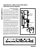
microprocessor (µP) port. Figure 1 shows the timing dia-
gram for signals on the 2-wire bus. Figure 2 shows the
typical application of the MAX520/MAX521. The 2-wire
bus can have several devices (in addition to the
MAX520/MAX521) attached. The two bus lines (SDA and
SCL) must be high when the bus is not in use. When in
use, the port bits are toggled to generate the appropriate
signals for SDA and SCL. External pull-up resistors are
not required on these lines. The MAX520/MAX521 can
be used in applications where pull-up resistors are
required (such as in I
2
C systems) to maintain compatibil-
ity with the existing circuitry.
The MAX520/MAX521 are receive-only devices and
must be controlled by a bus master device. They oper-
ate at SCL rates up to 400kHz. A master device sends
information to the devices by transmitting their address
over the bus and then transmitting the desired informa-
tion. Each transmission consists of a START condition,
the MAX520/MAX521’s programmable slave-address,
one or more command-byte/output-byte pairs (or a
command byte alone, if it is the last byte in the trans-
mission), and finally, a STOP condition (Figure 3).
The address byte and pairs of command and output
bytes are transmitted between the START and STOP con-
ditions. The SDA state is allowed to change only while
SCL is low. SDA’s state is sampled, and therefore must
remain stable while SCL is high. The only exceptions to
this are the START and STOP conditions. Data is transmit-
ted in 8-bit bytes. Nine clock cycles are required to trans-
fer the data bits to the MAX520/MAX521. Set SDA low
during the 9th clock cycle as the MAX520/MAX521 pull
SDA low during this time. R
C
(Figure 2) limits the current
that flows during this time if SDA stays high for short peri-
ods of time.
MAX520
SDA
R
C
1k
SCL
µC
REF0
SDA
SCL
AD1
AD0
+1V
QUAD
DAC
REF1
+4V
REF2
+5V
OFFSET ADJUSTMENT
REF3
OUT0
OFFSET ADJUSTMENT
GAIN ADJUSTMENT
GAIN ADJUSTMENT
OUT1
OUT2
OUT3
.
.
.
.
AD2
REF0
SDA
SCL
AD1
AD0
OCTAL
DAC
+5V
BRIGHTNESS ADJUSTMENT
REF4
OUT0
CONTRAST ADJUSTMENTOUT1
THRESHOLD
ADJUSTMENTS
OUT2
.
.
.
OUT6
OUT7
+5V
+5V
+12V
MOTOR
MAX521
Figure 2. Typical Application Circuit
START CONDITION
STOP CONDITION
OUTPUT BYTECOMMAND BYTE
SLAVE ADDRESS BYTE
SCL
SDA
MSB MSB MSBLSB LSB LSBACK ACK ACK
Figure 3. A Complete Serial Transmission