
Datasheet


MAX5181/MAX5184
10-Bit, 40MHz, Current/Voltage-Output DACs
_______________________________________________________________________________________ 9
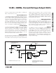
reference output-current resistor (R
SET
= 9.6kΩ) sets
I
REF
to 125µA and I
FS
to 1mA.
External Reference
To disable the MAX5181/MAX5184’s internal reference,
connect REN to DV
DD
. A temperature-stable, external
reference may now be applied to drive the REFO pin to
set the full-scale output (Figure 3). Choose a reference
capable of supplying at least 150µA to drive the bias
circuit that generates the cascode current for the cur-
rent array. For improved accuracy and drift perfor-
mance, choose a fixed output voltage reference such
as the 1.2V, 25ppm/°C MAX6520 bandgap reference.
Standby Mode
To enter the lower-power standby mode, connect digital
inputs PD and DACEN to DGND. In standby, both the
reference and the control amplifier are active with the
current array inactive. To exit this condition, DACEN
must be pulled high with PD held at DGND. The
MAX5181/MAX5184 typically require 50µs to wake up
and let both outputs and the reference settle.
Shutdown Mode
For lowest power consumption, the MAX5181/MAX5184
provide a power-down mode in which the reference, con-
trol amplifier, and current array are inactive and the DAC
supply current is reduced to 1µA. To enter this mode,
connect PD to DV
DD
. To return to active mode, connect
PD to DGND and DACEN to DV
DD
. About 50µs are
required for the parts to leave shutdown mode and settle
to their outputs’ values prior to shutdown. Table 1 lists the
power-down mode selection.
Timing Information
Figure 4 shows a detailed timing diagram for the
MAX5181/MAX5184. With each high transition of the
clock, the input latch is loaded with the digital value set
by bits D9 through D0. The content of the input latch is
then shifted to the DAC register, and the output up-
dates at the rising edge of the next clock.
Outputs
The MAX5181 output is designed to supply full-scale
output currents of 1mA into 400Ω loads in parallel with
a capacitive load of 5pF. The MAX5184 features inte-
grated 400Ω resistors that restore the array current to
proportional, differential voltages of 400mV. These dif-
ferential output voltages can then be used to drive a
balun transformer or a low-distortion, high-speed oper-
ational amplifier to convert the differential voltage into a
single-ended voltage.
R
SET
**
9.6kΩ
I
FS
R
SET
C
COMP
*
REFR
AGND
AGND
DGND
I
REF
REFO
MAX4040
R
SET
1.2V
BANDGAP
REFERENCE
REN
CURRENT-
SOURCE ARRAY
*COMPENSATION CAPACITOR (C
COMP
= 100nF) **9.6kΩ REFERENCE CURRENT-SET RESISTOR
INTERNAL TO MAX5184 ONLY. USE EXTERNAL
R
SET
FOR MAX5181.
OPTIONAL EXTERNAL BUFFER
FOR HEAVIER LOADS
MAX5181
MAX5184
Figure 2. Setting I
FS
with the Internal 1.2V Reference and the Control Amplifier