
Datasheet


MAX5175/MAX5177
Low-Power, Serial, 12-Bit DACs with
Force/Sense Voltage Output
______________________________________________________________________________________ 15
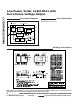
Using an AC Reference
The MAX5175/MAX5177 accept reference voltages
containing AC components, as long as the reference
voltage remains between 0 and V
DD
- 1.4V. Figure 10
shows a technique for applying a sine-wave signal to
REF. The reference voltage must remain above AGND.
Digitally Programmable
Current Source
The circuit of Figure 11 places an NPN transistor
(2N3904 or similar) within the op amp feedback loop to
implement a digitally programmable, unidirectional cur-
rent source. The output current is calculated with the
following equation:
where N is the numeric value of the DAC’s binary input
code and R is the sense resistor shown in Figure 11.
Power-Supply and Layout Considerations
Wire-wrap boards are not recommended. For optimum
system performance, use printed circuit boards with
separate analog and digital ground planes. Connect
the two ground planes together at the low-impedance
power-supply source. Connect DGND and AGND pins
together at the IC. The best ground connection is
achieved by connecting the DAC’s DGND and AGND
pins together and connecting that point to the system
analog ground plane. If the DAC’s DGND is connected
to the system digital ground, digital noise may infiltrate
the DAC’s analog portion.
Bypass the power supply with a 4.7µF capacitor in par-
allel with a 0.1µF capacitor to AGND. Minimize capaci-
tor lead lengths to reduce inductance. If noise
becomes an issue, use shielding and/or ferrite beads to
increase isolation.
In order to maintain INL and DNL performance, as well
as gain drift, it is extremely important to provide the
lowest possible reference output impedance at the
DAC reference input pin. INL degrades if the series
resistance on the REF pin exceeds 0.1Ω. The same
consideration must be made for the AGND pin.
DAC
OUT
MAX5175
MAX5177
R
1
R
1
REF
V
DD
GND
+5V/
+3.3V
+5V/+3.3V
AC
REFERENCE
INPUT
500mVp-p
MAX495
Figure 10. AC Reference Input Circuit
DAC
MAX5175
MAX5177
REF
OUT
R
I
OUT
2N3904
V
L
FB
+5V/+3.3V
V
DD
GND
Figure 11. Digitally Programmable Current Source
I
V N
R 4096
OUT
REF
=
⋅
⋅