
Datasheet


MAX5141–MAX5144
+3V/+5V, Serial-Input,
Voltage-Output, 14-Bit DACs
_______________________________________________________________________________________ 3
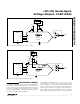
TIMING CHARACTERISTICS
(V
DD
= +2.7V to +3.3V (MAX5143/MAX5144), V
DD
= +4.5V to +5.5V (MAX5141/MAX5142), V
REF
= +2.5V, GND = 0, CMOS inputs,
T
A
= T
MIN
to T
MAX
, unless otherwise noted. Typical values are at T
A
= +25°C.) (Figure 1)
Note 1: Gain error tested at V
REF
= +2.0V, +2.5V, and +3.0V (MAX5143/MAX5144) or V
REF
= +2.0V, +2.5V, +3.0V, and +5.0V
(MAX5141/MAX5142).
Note 2: R
OUT
tolerance is typically ±20%.
Note 3: Min/max range guaranteed by gain-error test. Operation outside min/max limits will result in degraded performance.
Note 4: Reference input resistance is code dependent, minimum at 2155 hex in unipolar mode, 1155 hex in bipolar mode.
Note 5: Slew-rate value is measured from 10% to 90%.
Note 6: Guaranteed by design. Not production tested.
Note 7: Guaranteed by power-supply rejection test and Timing Characteristics.
Code = 3FFF hex
All digital inputs at
V
DD
or GND
All digital inputs at V
DD
or GND
MAX5143/MAX5144
Code = 0000 hex, V
REF
= 1V
P-P
at 100kHz
Code = 0000 hex
Code = 3FFF hex
(Note 6)
CONDITIONS
mW
0.36
PDPower Dissipation
mA0.12 0.20I
DD
Positive Supply Current
V
2.7 3.6
V
DD
Positive Supply Range (Note 7)
V0.15V
H
Hysteresis Voltage
pF310C
IN
Input Capacitance
mV
P-P
1
MHz1BWReference -3dB Bandwidth
µA±1I
IN
Input Current
V0.8V
IL
Input Low Voltage
V2.4V
IH
Input High Voltage
Reference Feedthrough
dB92SNRSignal-to-Noise Ratio
70
pF
170
C
INREF
Reference Input Capacitance
UNITSMIN TYP MAXSYMBOLPARAMETER
(Note 6)
CONDITIONS
µs20
V
DD
High to CS Low
(Power-Up Delay)
ns20t
CL
SCLK Pulse Width Low
ns20t
CH
MHz25f
CLK
SCLK Frequency
SCLK Pulse Width High
ns20t
CLW
CLR Pulse Width Low
ns0t
DH
DIN to SCLK High Hold
ns15t
DS
DIN to SCLK High Setup
ns15t
CSS0
CS Low to SCLK High Setup
ns15t
CSS1
CS High to SCLK High Setup
ns35t
CSH0
SCLK High to CS Low Hold
ns20t
CSH1
SCLK High to CS High Hold
UNITSMIN TYP MAXSYMBOLPARAMETER
ELECTRICAL CHARACTERISTICS (continued)
(V
DD
= +3V (MAX5143/MAX5144) or +5V (MAX5141/MAX5142), V
REF
= +2.5V, T
A
= T
MIN
to T
MAX
, C
L
= 10
p
F, GND = 0, RL = ∞,
unless otherwise noted. Typical values are at T
A
= +25°C.)
0.60MAX5141/MAX5142
MAX5143/MAX5144
MAX5141/MAX5142 4.5 5.5
DYNAMIC PERFORMANCE—REFERENCE SECTION
STATIC PERFORMANCE—DIGITAL INPUTS
POWER SUPPLY