
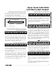
Datasheet


Serial Input Data Format and Control Codes
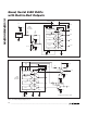
The 12-bit serial input format shown in Figure 3 com-
prises two DAC address bits (A1, A0), two control bits
(C1, C0) and eight bits of data (D0...D7).
The 4-bit address/control code configures the DAC as
shown in Table 1.
Load Input Register, DAC Registers Unchanged
(Single Update Operation)
When performing a single update operation, A1 and A0
select the respective input register. At the rising edge
of CS, the selected input register is loaded with the cur-
rent shift-register data. All DAC outputs remain
unchanged. This preloads individual data in the input
register without changing the DAC outputs.
Load Input and DAC Registers
This command directly loads the selected DAC register
at CS's rising edge. A1 and A0 set the DAC address.
Current shift-register data is placed in the selected
input and DAC registers.
For example, to load all four DAC registers simultaneously
with individual settings (DAC A = 1V, DAC B = 2V, DAC
C = 3V and DAC D = 4V), five commands are required.
First, perform four single input register update opera-
tions. Next, perform an “LDAC” command as a fifth
command. All DACs will be updated from their respec-
tive input registers at the rising edge of CS.
Update All DACs from Shift Registers
All four DAC registers are updated with shift-register
data. This command allows all DACs to be set to any
analog value within the reference range. This command
can be used to substitute CLR if code 00 hex is pro-
grammed, which clears all DACs.
No Operation (NOP)
The NOP command (no operation) allows data to be shift-
ed through the MAX509/MAX510 shift register without
affecting the input or DAC registers. This is useful in daisy
chaining (also see the
Daisy-Chaining Devices
section).
For this command, the data bits are "Don't Cares." As an
example, three MAX509/MAX510s are daisy-chained (A, B
and C), and DAC A and DAC C need to be updated. The
36-bit-wide command would consist of one 12-bit word for
device C, followed by an NOP instruction for device B and
a third 12-bit word with data for device A. At CS's rising
edge, only device B is not updated.
“LDAC” Command (Software)
All DAC registers are updated with the contents of their
respective input registers at CS's rising edge. With the
exception of using CS to execute, this performs the
same function as the asynchronous LDAC.
Set DOUT Phase – SCLK Rising (Mode 1, Default)
Mode 1 resets the serial output DOUT to transition at
SCLK's rising edge. This is the MAX509/MAX510’s
default setting after the supply voltage has been
applied.
The command also loads all DAC registers with the con-
tents of their respective input registers, and is identical to
the “LDAC” command.
MAX509/MAX510
Quad, Serial 8-Bit DACs
with Rail-to-Rail Outputs
______________________________________________________________________________________ 11
This is the first bit shifted in
A1 A0 C1 C0 D7 D6
● ● ●
D1 D0
DIN
DOUT
Control and
Address bits
8-bit DAC data
MSB
LSB
Figure 3. Serial Input Format
(LDAC = H)
(LDAC = x)
(LDAC = x)
(LDAC = x)
(LDAC = x)
(LDAC = H)
1 01 1 xxxxxxxx
D0D1D2D3D4D5D6D7C0
C1
A0
A1
8-Bit DAC Data0 0x 0
D0
D1D2D3D4D5D6D7
C0
C1
A0
A1
xxx xx xxx0 0x 1
D0D1D2D3D4D5D6D7C0
C1
A0
A1
1 00 x xx x xx x xx
D0D1D2D3D4D5D6D7C0
C1
A0
A1
8-Bit Data0 1Address
D0
D1D2D3D4D5D6D7
C0
C1
A0
A1
8-Bit Data1 1Address
D0
D1D2D3D4D5D6D7
C0
C1
A0
A1