
Datasheet


MAX509/MAX510
Quad, Serial 8-Bit DACs
with Rail-to-Rail Outputs
______________________________________________________________________________________ 17
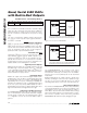
Figure 14. MAX509 AGND Bias Circuit (Negative Offset)
DAC A
DAC B
DAC C
DAC D
MAX509
OUTA
OUTB
OUTC
OUTD
SERIAL
INTERFACE
NOT SHOWN
REFERENCE INPUTS
2
1
20
19
V
DD
+5V
16
5174
18
3
-5V
8
V
SS
AGND
DGND
6
0.1μF
0.1μF
MAX873
+5V
0.1μF
R1
330k
0.1%
+5V
+2.5V
0.1μF
0.1μF
-5V
6
8
7
2
3
1
R2
330k
0.1%
ICL7611A
4-Quadrant Multiplication
Each DAC output may be configured for 4-quadrant
multiplication using Figure 16 and 17's circuit. One op
amp and two resistors are required per channel. With
R1 = R2:
V
OUT
= V
REF
[2(NB/256)-1]
where NB represents the digital word in DAC register A.
The recommended value for resistors R1 and R2 is
330kΩ (±0.1%). Table 3 shows the digital code vs. out-
put voltage for Figure 16 and 17's circuit.