
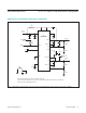
Datasheet


Design Guidelines
Input Capacitor (C
IN
) and
Boost Capacitor (C
BSOUT
) Selection
The input current waveform of the boost converter is con-
tinuous, and usually does not demand high capacitance
at its input. However, the MAX5092_/MAX5093_ boost
converter is designed to fully turn on as soon as the input
drops below a certain voltage in order to ride out cold-
crank droops. This operation demands low input source
impedance for proper operation. If the source (battery) is
located far from the IC, high-capacity, low-ESR capacitors
are recommended for C
IN
. The worst-case peak capacitor
current could be as high as 3A. Use a 47μF, 100mΩ low-
ESR capacitor placed as close as possible to the input of
the device. Note that the aluminum electrolytic capacitor
ESR increases significantly at cold temperatures. In the
cold temperature case, choose an electrolyte capacitor
with ESR lower than 40mΩ or connect a low-ESR ceramic
capacitor (10μF) in parallel with the electrolytic capacitor.
The boost converter output (BSOUT) is fed to the input of
the internal 250mA LDO. The boost-converter output cur-
rent waveform is discontinuous and requires highcapacity,
low-ESR capacitors at BSOUT to ensure low V
BSOUT
ripple. During the on-time of the internal MOSFET, the
BSOUT capacitor supplies 250mA current to the LDO
input. During the off-time, the inductor dumps current
into the output capacitor while supplying the output load
current. The internal 250mA LDO is designed with high
PSRR; however, high-frequency spikes may not be reject-
ed by the LDO. Thus, high-value, low-ESR electrolytic
capacitors are recommended for C
BSOUT
. Peak-to-peak
V
BSOUT
ripple depends on the ESR of the electrolyte
capacitor. Use the following equation to calculate the
required ESR (ESR
BSOUT
) of the BSOUT capacitor:
ESRBS
BSOUT
LIM OUT
V
ESR
II
−
∆
=
where ΔV
ESRBS
is 75% of total peak-to-peak ripple at
BSOUT, I
LIM
is the internal switch current limit (3A max),
and I
OUT
is the LDO output current. Use a 100mΩ or
lower ESR electrolytic capacitor. Make sure the ESR at
cold temperatures does not cause excessive ripple volt-
age. Alternately, use a 10μF ceramic capacitor in parallel
with the electrolyte capacitor.
During the switch on-time, the BSOUT capacitor dis-
charges while supplying I
OUT
. The ripple caused by the
capacitor discharge (ΔV
CBS
) is estimated by using the
following equation:
6
OUT
CBS
BSOUT
I 2.7 10
V
C
−
××
∆=
where I
OUT
is the LDO output current and C
BSOUT
is the
BSOUT capacitance.
Inductor Selection
The control scheme of the MAX5092/MAX5093 permits
flexibility in choosing an inductor value. Smaller induc-
tance values typically offer smaller physical size for a
given series resistance, allowing the smallest overall
circuit dimensions. Circuits using larger inductance may
provide higher efficiency and exhibit less ripple, but also
may reduce the maximum output current. This occurs
when the inductance is sufficiently large to prevent the LX
current limit (I
LIM
) from being reached before the maxi-
mum on-time (t
ON-MAX
) expires.
For maximum output current, choose the inductor value
so that the controller reaches the current limit before the
maximum on-time is reached:
IN ON MAX
LIM
Vt
L
I
−
×
≤
where t
ON-MAX
is typically 2.25μs, and the current
limit (I
LIM
) is a maximum of 3A (see the Electrical
Characteristics). Choose an inductor with the maximum
saturation current (I
SAT
) greater than 3A.
MAX5092/MAX5093 4V to 72V Input LDOs with Boost Preregulator
www.maximintegrated.com
Maxim Integrated
│
18