
Datasheet


MAX5072
2.2MHz, Dual-Output Buck or Boost
Converter with POR and Power-Fail Output
______________________________________________________________________________________ 25
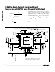
Layout Procedure
1) Place the power components first, with ground ter-
minals adjacent (inductor, C
IN_
, and C
OUT_
). Make
all these connections on the top layer with wide,
copper-filled areas (2oz copper recommended).
2) Group the gate-drive components (bootstrap
diodes and capacitors, and VL bypass capacitor)
together near the controller IC.
3) Make the DC-DC controller ground connections as
follows:
a) Create a small-signal ground plane underneath
the IC.
b)Connect this plane to SGND and use this plane
for the ground connection for the reference
(BYPASS), enable, compensation components,
feedback dividers, and OSC resistor.
c) Connect SGND and PGND together near the
input bypass capacitors and the IC (this is the
only connection between SGND and PGND).
Chip Information
TRANSISTOR COUNT: 5994
PROCESS: BiCMOS
Ordering Information (continued)
*EP = Exposed pad.
+Denotes lead-free package.
PART
TEMP RANGE
PIN-PACKAGE
PKG
CODE
M AX5072E TJ+
-40°C to +85°C
32 Thin QFN-EP*
(5mm x 5mm)
T3255-4
MAX5072ATJ
-40°C to +125°C
32 Thin QFN-EP*
(5mm x 5mm)
T3255-4
M AX5072ATJ+
-40°C to +125°C
32 Thin QFN-EP*
(5mm x 5mm)
T3255-4