
Datasheet


MAX4575/MAX4576/MAX4577
±15kV ESD-Protected, Low-Voltage, Dual, SPST,
CMOS Analog Switches
8 _______________________________________________________________________________________
and bypass the surge safely to ground. This method is
superior to using diode clamps to the supplies
because, unless the supplies are very carefully decou-
pled through low-ESR capacitors, the ESD current
through the diode clamp could cause a significant
spike in the supplies. This may damage or compromise
the reliability of any other chip powered by those same
supplies.
There are diodes from NC/NO to the supplies in addi-
tion to the SCRs. There is a resistance in series with
each of these diodes to limit the current into the sup-
plies during an ESD strike. The diodes protect these
terminals from overvoltages that are not a result of ESD
strikes. These diodes also protect the device from
improper power-supply sequencing.
Once the SCR turns on because of an ESD strike, it
continues to be on until the current through it falls
below its “holding current.” The holding current is typi-
cally 110mA in the positive direction (current flowing
into the NC/NO terminal) at room temperature (see SCR
Holding Current vs. Temperature in the Typical
Operating Characteristics). Design the system so that
any sources connected to NC/NO are current limited to
a value below the holding current to ensure the SCR
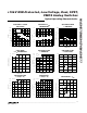
Figure 5. Crosstalk
SIGNAL
GENERATOR 0dBm
V+
10nF
ANALYZER
NO2/NC2
R
L
GND
COM1
0 OR 2.4V
IN1
NO1/NC1
50Ω
COM2
IN2
0 OR
2.4V
NC
V+
MAX4575
MAX4576
MAX4577
Figure 4. Channel Off/On-Capacitance
CAPACITANCE
METER
NO_/NC_
COM
GND
IN
10nF
V+
f = 1MHz
V+
MAX4575
MAX4576
MAX4577
V
IL
OR
V
IH
V
GEN
GND
NO_/NC_
C
L
V
OUT
V+
V
OUT
∆V
OUT
Q = (∆V
OUT
)(C
L
)
COM
OFF
ON
OFF
IN
V
IN
V+
R
GEN
IN
MAX4575
MAX4576
MAX4577
Figure 3. Charge Injection