
Datasheet


V+ Supply Current
MAX4545/MAX4546/MAX4547
Quad/Dual, Low-Voltage,
Bidirectional RF/Video Switches
_______________________________________________________________________________________ 5
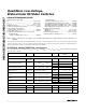
ELECTRICAL CHARACTERISTICS—Single +3V Supply
(V+ = +2.7V to +3.6V, V- = 0V, V
INL
= 0.8V, V
INH
= 2.4V, V
GND_
= 0V, T
A
= T
MIN
to T
MAX
, unless otherwise noted. Typical values are
at T
A
= +25°C.)
V+ = 2.7V, V
COM_
= 1V,
I
COM_
= 1mA
(Note 3)
V+ = 3.6V, all V
IN_
= 0V or V+
V
COM_
= 1.5V, V+ = 2.7V,
Figure 4 (Note 3)
V
COM_
= 1.5V, V+ = 2.7V,
Figure 5 (Note 3)
V
IN_
= 0.8V or 2.4V (Note 3)
(Note 3)
(Note 3)
V
COM_
= 1.5V, V+ = 2.7V,
Figure 4 (Note 3)
CONDITIONS
µA
-1 0.05 1
I+V+ Supply Current
ns15 100t
BBM
Break-Before-Make Time Delay
(MAX4546/MAX4547 only)
ns
200
50 150
t
OFF
Turn-Off Time
70 120
R
ON
Signal-Path On-Resistance
V0 V+
V
COM_
,
V
NO_
, V
NC_
Analog Signal Range
ns
800
300 600
t
ON
Turn-On Time
µA-1 1I
INH_
, I
INL_
IN_ Input Current Logic High or
Low
Ω
150
V1.0 2.4V
IN_H
IN_ Input Logic Threshold High
V0.8 1.0V
IN_L
IN_ Input Logic Threshold Low
UNITS
MIN TYP MAX
(Note 2)
SYMBOLPARAMETER
+25°C
+25°C
+25°C
C, E
+25°C
+25°C
C, E
C, E
C, E
C, E
C, E
+25°C
T
A
-10 10C, E
ANALOG SWITCH
LOGIC INPUT
SWITCH DYNAMIC CHARACTERISTICS
POWER SUPPLY
Note 2: The algebraic convention is used in this data sheet; the most negative value is shown in the minimum column.
Note 3: Guaranteed by design.
Note 4: ∆R
ON
= ∆R
ON(MAX)
- ∆R
ON(MIN)
.
Note 5: Resistance flatness is defined as the difference between the maximum and the minimum value of on-resistance as mea-
sured over the specified analog signal range.
Note 6: Leakage parameters are 100% tested at the maximum rated hot temperature and guaranteed by correlation at +25°C.
Note 7: Off isolation = 20log
10
[V
COM
/ (V
NC
or V
NO
)], V
COM
= output, V
NC
or V
NO
= input to off switch.
Note 8: Between any two switches.
Note 9: Leakage testing for single-supply operation is guaranteed by testing with dual supplies.