
Datasheet


MAX4524/MAX4525
Low-Voltage, Single-Supply
Multiplexer and Switch
4 _______________________________________________________________________________________
Note 2: The algebraic convention is used in this data sheet; the most negative value is shown in the minimum column.
Note 3: ∆R
ON
= R
ON(MAX)
- R
ON(MIN)
Note 4: Flatness is defined as the difference between the maximum and minimum value of on-resistance as measured over the
specified analog signal ranges; i.e., V
NO
= 3V to 0V and 0V to 3V.
Note 5: Leakage parameters are 100% tested at maximum-rated hot operating temperature, and guaranteed by correlation at
T
A
= +25°C.
Note 6: Guaranteed by design, not production tested.
Note 7: TDFN parts are tested at +25°C and are guaranteed by design and correlation over the entire temperature range.
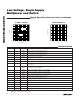
ELECTRICAL CHARACTERISTICS—Single +3V Supply (continued)
(V+ = 2.7V to 3.6V, GND = 0V, V
AH
= 2.0V, V
AL
= 0.5V, T
A
= T
MIN
to T
MAX
, unless otherwise noted. Typical values are at
T
A
= +25°C.) (Notes 2, 7)
V
A
= V
INH
= 2.0V
V
A
= V
INH
= 0.5V
CONDITIONS
+25°C
V1.0 2.0V
IH
Logic Input Logic
Threshold High
C, E
µA-1 +1I
IH
Input Current Low
-2 +2
µA-1 +1I
IH
Input Current High
UNITS
MIN TYP MAX
(Note 2)
SYMBOLPARAMETER
V0.5 1.0V
IL
Logic Input Logic
Threshold Low
C, E
C, E
TEMP
C, E
170 300+25°C
V
NO_
= 1.5V, R
L
= 300Ω, C
L
= 35pF,
Figure 2
50 200
ns
400
t
(ON)
Inhibit Turn-On Time
C, E
+25°C
V
NO_
= 1.5V, R
L
= 300Ω, C
L
= 35pF,
Figure 2
130 300
ns
300
t
(OFF)
Inhibit Turn-Off Time
C, E
+25°C
V
NO_
= 1.5V/0V, R
L
= 300Ω, C
L
= 35pF,
Figure 1
ns
400
t
TRANS
Address Transition Time
C, E
Figure 3, V
NO_
= 1.5V, R
L
= 300Ω, C
L
= 35pF ns540t
BBM
Break-Before-Make Time +25°C
-1 +1+25°C
V+ = 3.6V, V
ADD
= V
INH
= V+ or 0V µA
-10 +10
I+Power-Supply Current
C, E
C, E -50 +50
V+ = 3.6V; V
COM
= 3V, 1V
C, E
nA
-25 +25
I
COM(ON)
COM On-Leakage
(Note 6)
+25°C -1 +1
MAX4524
MAX4525
DIGITAL I/O
SWITCH DYNAMIC CHARACTERISTICS (Note 6)
POWER SUPPLY