
Datasheet


MAX4265–MAX4270
Ultra-Low-Distortion, +5V,
400MHz Op Amps with Disable
14 ______________________________________________________________________________________
5
-5
0.1M 1M 10M 100M 1G
-3
FREQUENCY (Hz)
GAIN (dB)
-1
1
3
2
0
-2
-4
4
C
L
= 2.2pF
C
L
= 5.1pF
C
L
= 7.3pF
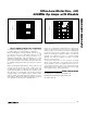
Figure 3a. MAX4268 Small-Signal Gain vs. Frequency
Without Isolation Resistor
5
-5
0.1M 1M 10M 100M 1G
-3
FREQUENCY (Hz)
GAIN (dB)
-1
1
3
2
0
-2
-4
4
C
L
= 2.2pF
C
L
= 5.1pF
C
L
= 7.3pF
Figure 3b. MAX4269 Small-Signal Gain vs. Frequency
Without Isolation Resistor
4
-6
0.1M 1M 10M 100M 1G
-4
FREQUENCY (Hz)
GAIN (dB)
-2
0
2
1
-1
-3
-5
3
C
L
= 10pF
C
L
= 15pF
C
L
= 7.3pF
Figure 3c. MAX4270 Small-Signal Gain vs. Frequency
Without Isolation Resistor
5
-5
0.1M 1M 10M 100M 1G
-3
FREQUENCY (Hz)
GAIN (dB)
-1
1
3
2
0
-2
-4
4
C
L
= 10pF
R
ISO
= 12Ω
C
L
= 10pF
R
ISO
= 15Ω
C
L
= 10pF
R
ISO
= 18Ω
Figure 4a. MAX4268 Small-Signal Gain vs. Frequency
With Isolation Resistor
be maintained using an amplifier with very low output
impedance at high frequencies. The combination of
high speed, fast slew rate, low noise, and a low and
stable distortion overload makes the MAX4265–
MAX4270 ideally suited for use as buffer amplifiers in
high-speed ADC applications.
Low-Power Disable Mode
The MAX4265–MAX4270 feature an active-low disable
mode that can be used to save power and place the
outputs in a high-impedance state. Drive DISABLE_ with
logic levels, or connect DISABLE_ to V
CC
for normal
operation. In the dual versions (MAX4268/ MAX4269/
MAX4270), each individual op amp is disabled sepa-
rately, allowing the devices to be used in a multiplex
configuration. The supply current in low-power mode is
reduced to 1.6mA per amplifier. Enable time is typically
100ns, and disable time is typically 750µs.
20
15
10
5
0
06020 40 80 100 120
C
LOAD
(pF)
R
ISO
(Ω)
MAX4265/MAX4268
MAX4266/MAX4269
MAX4267/MAX4270
Figure 2. MAX4265–MAX4270 Isolation Resistance vs.
Capacitive Load