
Datasheet


MAX4210/MAX4211
High-Side Power and
Current Monitors
2 _______________________________________________________________________________________
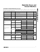
ABSOLUTE MAXIMUM RATINGS
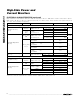
ELECTRICAL CHARACTERISTICS
(V
CC
= 5.0V, V
RS+
= 25V, V
SENSE
= 5mV, V
IN
= 1.0V, V
LE
= 0V, R
IOUT
= R
POUT
= 1MΩ, V
CIN1+
= V
CIN2+
= V
REF
, V
CIN1-
= V
CIN2-
=
GND, V
INHIBIT
= 0V, R
COUT1
= R
COUT2
= 5kΩ connected to V
CC
, T
A
= -40°C to +85°C, unless otherwise noted. Typical values are at
T
A
= +25°C, unless otherwise noted.) (Note 1)
Stresses beyond those listed under “Absolute Maximum Ratings” may cause permanent damage to the device. These are stress ratings only, and functional
operation of the device at these or any other conditions beyond those indicated in the operational sections of the specifications is not implied. Exposure to
absolute maximum rating conditions for extended periods may affect device reliability.
V
CC
, IN, CIN1, CIN2 to GND....................................-0.3V to +6V
RS+, RS-, INHIBIT, LE, COUT1, COUT2 to GND ...-0.3V to +30V
IOUT, POUT, REF to GND..........................-0.3V to (V
CC
+ 0.3V)
Differential Input Voltage (V
RS+
- V
RS-
) .................................±5V
Maximum Current into Any Pin..........................................±10mA
Output Short-Circuit Duration to V
CC
or GND ........................10s
Continuous Power Dissipation (T
A
= +70°C)
6-Pin TDFN (derate 24.4mW/°C above +70°C) ..........1951mW
8-Pin µMAX (derate 4.5mW/°C above +70°C) .............362mW
16-Pin TSSOP (derate 9.4mW/°C above +70°C) ..........754mW
16-Pin Thin QFN (derate 25mW/°C above +70°C) .....2000mW
Operating Temperature Range ...........................-40°C to +85°C
Junction Temperature......................................................+150°C
Storage Temperature Range .............................-65°C to +150°C
Lead Temperature (soldering, 10s) .................................+300°C
PARAMETER SYMBOL CONDITIONS
MIN
TYP
MAX
UNITS
Operating Voltage Range
(Note 2)
V
CC
2.7 5.5 V
Common-Mode Input Range
(Note 3)
V
CMR
Measured at RS+ 4 28 V
MAX4210
380 570
T
A
= +25°C,
V
CC
= +5.5V
MAX4211
670 960
MAX4210
670
Supply Current I
CC
V
CC
= +5.5V
MAX4211
1100
µA
MAX421_A/B/C 14 25
I
RS+
V
SENSE
= 0mV
MAX421_D/E/F 3 8
Input Bias Current
I
RS-
V
SENSE
= 0mV 3 8
µA
IN Input Bias Current I
IN
MAX421_D/E/F
-0.1
-1 µA
Leakage Current I
RS+
, I
RS-
V
CC
= 0V 0.1 1 µA
MAX421_A/B/D/E 150
V
SENSE
Full-Scale Voltage
(Note 4)
V
SENSE_FS
MAX421_C/F 100
mV
IN Full-Scale Voltage
(Note 4)
V
IN_FS
MAX421_D/E/F, V
SENSE
= 10mV to
100mV
1V
IN Input Voltage Range
(Note 5)
V
IN
MAX421_D/E/F, V
SENSE
= 10mV to
100mV
0.16 1.10
V
V
RS+
Full-Scale Voltage
(Note 4)
MAX421_A/B/C, V
SENSE
= 10mV to
100mV
25 V
V
RS+
Input Voltage Range
(Note 5)
V
RS+
MAX421_A/B/C, V
SENSE
= 10mV to
100mV
428V
Current into IOUT = 10µA
1.5
Current into IOUT = 100µA
2.5 80
Current into POUT = 10µA
1.5
Minimum IOUT/POUT Voltage V
OUT_MIN
V
SENSE
=
0V, V
RS+
=
25V
C ur r ent i nto P O U T = 100µA
2.5 80
mV
Current out of
IOUT = 500µA
V
CC
-
0.25
Maximum IOUT/POUT Voltage
(Note 6)
V
OUT_MAX
V
SENSE
=
300mV,
V
RS+
= 25V
Current out of
POUT = 500µA
V
CC
-
0.25
V