
Datasheet


MAX410/MAX412/MAX414
Single/Dual/Quad, 28MHz, Low-Noise,
Low-Voltage, Precision Op Amps
10 ______________________________________________________________________________________
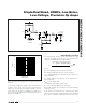
Tech measures input-referred noise. For the circuit in
Figure 5, assuming R
p
is approximately equal to R
n
and the measurement is taken with the Quan Tech
model 5173, the equation simplifies to:
Input Protection
To protect amplifier inputs from excessive differential
input voltages, most modern op amps contain input
protection diodes and current-limiting resistors. These
resistors increase the amplifier’s input-referred noise.
They have not been included in the MAX410/MAX412/
MAX414, to optimize noise performance. The MAX410/
MAX412/MAX414 do contain back-to-back input pro-
tection diodes which will protect the amplifier for differ-
ential input voltages of ±0.1V. If the amplifier must be
protected from higher differential input voltages, add
external current-limiting resistors in series with the op
amp inputs to limit the potential input current to less
than 20mA.
Capacitive-Load Driving
Driving large capacitive loads increases the likelihood
of oscillation in amplifier circuits. This is especially true
for circuits with high loop gains, like voltage followers.
The output impedance of the amplifier and a capacitive
load form an RC network that adds a pole to the loop
response. If the pole frequency is low enough, as when
driving a large capacitive load, the circuit phase mar-
gin is degraded.
In voltage follower circuits, the MAX410/MAX412/
MAX414 remain stable while driving capacitive loads
as great as 3900pF (see Figures 6a and 6b).
When driving capacitive loads greater than 3900pF,
add an output isolation resistor to the voltage follower
circuit, as shown in Figure 7a. This resistor isolates the
load capacitance from the amplifier output and restores
the phase margin. Figure 7b is a photograph of the
response of a MAX410/MAX412/MAX414 driving a
0.015µF load with a 10Ω isolation resistor
The capacitive-load driving performance of the
MAX410/MAX412/MAX414 is plotted for closed-loop
gains of -1V/V and -10V/V in the % Overshoot vs.
Capacitive Load graph in the
Typical Operating
Characteristics
.
Feedback around the isolation resistor RI increases the
accuracy at the capacitively loaded output (see Figure 8).
The MAX410/MAX412/MAX414 are stable with a 0.01µF
load for the values of R
I
and C
F
shown. In general, for
decreased closed-loop gain, increase R
I
or C
F
. To drive
larger capacitive loads, increase the value of C
F
.
i
e
AHz
n
no
2
-20 3
3
- (1.64 10 )(20 10 )
(20 10 )
=
××
[]
×
/
Figure 5. Current-Noise Test Circuit
100Ω
909Ω
+5V
0.022µF
R
p
10kΩ
D.U.T
-5V
e
no
MAX410
MAX412
MAX414
R
n
10kΩ
0.022µF
Figure 6a. Voltage Follower Circuit with 3900pF Load
R
f
499Ω
D.U.T
V
OUT
MAX410
MAX412
MAX414
3900pF
V
IN
Figure 6b. Driving 3900pF Load as Shown in Figure 6a
1µs/div
INPUT
1V/div
OUTPUT
1V/div
GND
GND
V
S
= ±5V
T
A
= +25°C