
Datasheet


MAX4051/A, MAX4052/A, MAX4053/A
Low-Voltage, CMOS Analog
Multiplexers/Switches
10 ______________________________________________________________________________________
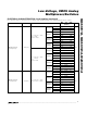
____________________________Typical Operating Characteristics (continued)
(V+ = +5V, V- = -5V, GND = 0V, T
A
= +25°C, unless otherwise noted.)
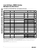
_____________________________________________________________Pin Descriptions
Digital Inhibit Input. Normally connect to GND. Can be driven
to logic high to set all switches off.
66
Negative Analog Supply Voltage Input. Connect to GND for
single-supply operation.
77
Ground. Connect to digital ground. (Analog signals have no
ground reference; they are limited to V+ and V-.)
88
Digital Address “C” Input—9
Digital Address “B” Input910
Analog Switch “B” Normally Open Input——
Analog Switch “B” Normally Closed Input——
Analog Switch “A” Normally Open Input——
Analog Switch “A” Normally Closed Input——
Analog Switch “B” Common3—
Analog Switch “B” Inputs 0–31, 2, 4, 5—
Analog Switch Common—3
Analog Switch Inputs 0–7—
1, 2, 4, 5, 12,
13, 14, 15
FUNCTION
Analog Switch “C” Normally Closed Input——
Analog Switch “C” Normally Open Input——
Analog Switch “C” Common——
Digital Address “A” Input1011
Analog Switch “A” Inputs 0–311, 12, 14, 15—
Analog Switch “A” Common13—
Note: NO, NC, and COM pins are identical and interchangeable. Any may be considered an input or output; signals pass equally
well in both directions.
INH
6
V-7
GND8
ADDC11
ADDB10
NOB1
NCB2
NOA3
NCA5
COMB15
NO0B–NO3B—
COM—
NO0–NO7—
NAME
NCC12
NOC13
COMC14
ADDA9
NO0A–NO3A—
COMA4
MAX4051/
MAX4051A
MAX4052/
MAX4052A
MAX4053/
MAX4053A
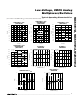
0.01
10 100 1k 10k
TOTAL HARMONIC DISTORTION
vs. FREQUENCY
0.1
MAX4051/2/3-10
FREQUENCY (Hz)
THD (%)
1
10
100
V± = ±5V
600
Ω
IN AND OUT
Positive Analog and Digital Supply Voltage Input1616 V+16
PIN
0
-10
-90
0.01 0.1 1 10 100 300
FREQUENCY RESPONSE
-80
-70
MAX4051/2/3-09
FREQUENCY (MHz)
LOSS (dB)
PHASE (DEGREES)
-50
-60
-40
-20
-30
5
0
-40
-35
-30
-20
-25
-15
-5
-10
INSERTION LOSS
50Ω IN/OUT
OFF-ISOLATION
ON PHASE