
Datasheet


MAX3984
1Gbps to 10Gbps Preemphasis Driver with
Receive Equalizer
_______________________________________________________________________________________ 3
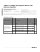
PARAMETER SYMBOL CONDITIONS MIN TYP MAX UNITS
OUT_LEV = low, TX_DISABLE = low 100 124
Supply Current I
CC
OUT_LEV = high, TX_DISABLE = low 120 148
mA
Inrush Current Beyond steady state supply current (Note 1) 10 mA
Power-On Delay (Note 1) 1 30 ms
EQUALIZER AND DRIVE SPECIFICATIONS
Input Return Loss S11 100MHz to 5GHz 10 dB
Input Resistance Measured differentially (Note 2) 85 100 115
Measured differentially at point B in Figure
2; TX_DISABLE = low, OUT_LEV = high,
PE1 = PE0 = high
1000 1300
Measured differentially at point B in Figure
2; TX_DISABLE = low, OUT_LEV = low,
PE1 = PE0 = high
800 1100
Different Output Swing
(Notes 3, 4)
TX_DISABLE = high, PE1 = PE0 = high 10
mV
P-P
Common-Mode Output (AC)
(Note 4)
Measured at point B in Figure 2;
TX_DISABLE = low, OUT_LEV = high (Note 5)
25 mV
RMS
Output Resistance R
OUT
OUT+ or OUT-, single-ended 42 50 58
Output Return Loss S22 100MHz to 5GHz 12 dB
Output Transition Time 20%
to 80%
t
r
, t
f
20% to 80% (Note 6) 32 40 ps
Random Jitter (Note 4) Measured at point D in Figure 3 (Note 7) 0.8 ps
RMS
PE1 PE0
0 0 3.5
0 1 6.5
1 0 9.5
Output Preemphasis Figure 1 (Note 3)
1 1 13
dB
Source to IN
OUT to
load
PE1 PE0
3m,
24 AWG
0 0
5m,
24 AWG
0 1
7m,
24 AWG
1 0
Residual Output Deterministic
Jitter at 1.0Gbps
(Notes 4, 8, and 9)
6-mil, 10in of
FR-4
10m,
24 AWG
1 1
0.02 UI
P-P
ELECTRICAL CHARACTERISTICS
(V
CC
= +3.0V to +3.6V, T
A
= 0°C to +85°C. Typical values are at T
A
= +25°C, V
CC
= +3.3V, unless otherwise noted.)