
Datasheet


MAX3984
1Gbps to 10Gbps Preemphasis Driver with
Receive Equalizer
2 _______________________________________________________________________________________
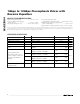
ABSOLUTE MAXIMUM RATINGS
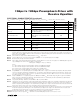
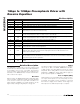
OPERATING CONDITIONS
Stresses beyond those listed under “Absolute Maximum Ratings” may cause permanent damage to the device. These are stress ratings only, and functional
operation of the device at these or any other conditions beyond those indicated in the operational sections of the specifications is not implied. Exposure to
absolute maximum rating conditions for extended periods may affect device reliability.
Supply Voltage Range (V
CC
).................................-0.5V to +4.1V
Continuous Output Current Range
(OUT+, OUT-) ...............................................-25mA to +25mA
Input Voltage Range (IN+, IN-) ..................-0.5V to (V
CC
+ 0.5V)
Logic Inputs Range (PE1, PE0,
TX_DISABLE, IN_LEV, OUT_LEV) ..........-0.5V to (V
CC
+ 0.5V)
LOS Open-Collector Supply Voltage Range
(with ≥ 4.7kΩ pullup) .........................................-0.5V to +5.5V
Storage Ambient Temperature Range (T
STG
) ...-55°C to +150°C
PARAMETER SYMBOL CONDITIONS MIN TYP MAX UNITS
Supply Voltage V
CC
3.0 3.3 3.6 V
Supply Noise Tolerance 1MHz f < 2GHz 40 mV
P-P
Operating Ambient Temperature T
A
0 25 85 °C
Bit Rate NRZ data 1.0 8.5 10.3 Gbps
Consecutive Identical Digits
(CID)
CID (bits) 100 Bits
IN_LEV = high, Figure 2;
4.25Gbps < data rate 10.3Gbps
360 1200
IN_LEV = high, Figure 2;
1.25Gbps < data rate 4.25Gbps
360 1600
IN_LEV = high, Figure 2;
1.0Gbps data rate 1.25Gbps
360 2400
Input Swing (Measured
differentially at data source,
point A of Figure 2 and 3. Pins
LOS and TX_DISABLE are
floating.)
IN_LEV = low, Figure 3;
1.0Gbps < data rate 10.3Gbps
100 360
mV
P-P
Time to Reach 50%
Mark/Space Ratio
1 μs