
Datasheet


MAX3980
Detailed Description
Receiver and Transmitter
The receiver accepts four lanes of 3.125Gbps current-
mode logic (CML) digital data signals. The adaptive
equalizer compensates each received signal for dielec-
tric and skin losses. The limiting amp shapes the output
of the equalizer. The regenerated XAUI lanes are trans-
mitted as CML signals. The source impedance and ter-
mination impedances are 100Ω differential.
General Theory of Operation
Internally, the MAX3980 comprises signal-detect cir-
cuitry, four matched equalizers, and one equalizer-
control loop. The four equalizers are made up of a mas-
ter equalizer and three slave equalizers. The adaptive
control is generated from only channel 1. It is assumed
that all channels have the same characterization in fre-
quency content, coding, and transmission length.
The master equalizer consists of the following functions:
signal detect, adaptive equalizer, equalizer control, and
limiting and output drivers. The signal detect indicates
input signal power. When the input signal level is suffi-
ciently high, the SDET output is asserted. This does not
directly control the operation of the part.
The equalizer core reduces intersymbol interference
(ISI), compensating for frequency-dependent, media-
induced loss. The equalization control detects the
spectral contents of the input signal and provides a
control voltage to the equalizer core, adapting it to dif-
ferent media. The equalizer operation is optimized for
short-run DC-balanced transmission codes such as
8b/10b codes.
CML Input and Output Buffers
The input and output buffers are implemented using
CML. Equivalent circuits are shown in Figures 2 and 3.
For details on interfacing with CML, see Maxim applica-
tion note HFAN-1.0,
Interfacing Between CML, PECL,
and LVDS
. The common-mode voltage of the input and
output is above 2.5V. AC-coupling capacitors are
required when interfacing this part. Values of 0.10µF or
greater are recommended.
Media Equalization
Equalization at the input port compensates for the high-
frequency loss encountered with up to 40in (1.0m) of
FR-4 transmission lines. This part is optimized for 40in
and 3.125Gbps; however, the part reduces ISI for sig-
nals spanning longer distances and functions for data
rates from 2Gbps to 4Gbps, provided that short-length
balanced codes, such as 8b/10b, are used.
Applications Information
Standby Mode
The power-saver standby state allows reduced-power
operation. The TTL input, EN, must be set to TTL high
for normal operation. A TTL low at EN forces the equal-
izer into the standby state. The signal EN does not
affect the operation of the signal detect (SDET) func-
tion. For constant operation, connect the EN signal
directly to V
CC
.
3.125Gbps XAUI Quad Equalizer
6 _______________________________________________________________________________________
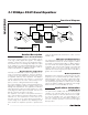
Functional Diagram
IN1+
IN1-
EQUALIZER
LIMITING
AMP
2
3
4
2
3
4
2
3
4
2
3
4
2
3
4
2
3
4
OUT1+
OUT1-
2
3
4
2
3
4
EN
POWER
MANAGEMENT
SDET FUNCTION IS
INDEPENDENT OF EN
SDET
TTL
CML
SIGNAL
DETECT
IP1, IN1 ONLY
MAX3980