
Datasheet


MAX3738
155Mbps to 4.25Gbps SFF/SFP Laser Driver
with Extinction Ratio Control
8 _______________________________________________________________________________________
Detailed Description
The MAX3738 laser driver consists of three main parts:
a high-speed modulation driver, biasing block with
ERC, and safety circuitry. The circuit design is opti-
mized for high-speed, low-voltage (+3.3V) operation
(Figure 4).
High-Speed Modulation Driver
The output stage is composed of a high-speed differ-
ential pair and a programmable modulation current
source. The MAX3738 is optimized for driving a 15Ω
load. The minimum instantaneous voltage required at
OUT- is 0.7V for modulation currents up to 60mA and
0.75V for currents from 60mA to 85mA. Operation
above 60mA can be accomplished by AC-coupling or
with sufficient voltage at the laser to meet the driver
output voltage requirement.
To interface with the laser diode, a damping resistor
(R
D
) is required. The combined resistance damping
resistor and the equivalent series resistance (ESR) of
the laser diode should equal 15Ω. To further damp
aberrations caused by laser diode parasitic induc-
tance, an RC shunt network may be necessary. Refer to
Application Note 274:
HFAN-02.0: Interfacing Maxim
Laser Drivers with Laser Diodes
for more information.
At high data rates, any capacitive load at the cathode of
a laser diode degrades optical output performance.
Because the BIAS output is directly connected to the
laser cathode, minimize the parasitic capacitance asso-
ciated with the pin by using an inductor to isolate the
BIAS pin parasitics from the laser cathode.
Extinction Ratio Control
The extinction ratio (r
e
) is the laser on-state power
divided by the off-state power. Extinction ratio remains
constant if peak-to-peak and average power are held
constant:
r
e
= (2P
AVG
+ P
P-P
) / (2P
AVG
- P
P-P
)
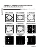
V
IN+
V
IN-
200mV (min)
2400mV (max)
100mV (min)
1200mV (max)
I
MOD
VOLTAGE
CURRENT
TIME
SINGLE ENDED
DIFFERENTIAL
(V
IN+
) - (V
IN-
)
I
OUT+
Figure 1. Required Input Signal and Output Polarity
MAX3738
OUT+
OUT-
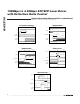
OSCILLOSCOPE
BIAS-T
BIAS-T
21Ω
50Ω 50Ω21Ω
1μF
1
μ
F
Figure 2. Test Circuit for Characterization
L1
1μH
C1
0.1μF
C3
0.1μF
C2
10μF
VOLTAGE
SUPPLY
SOURCE
NOISE
OPTIONAL
OPTIONAL
FILTER DEFINED BY SFP MSA
HOST BOARD
MODULE
TO LASER
DRIVER V
CC
Figure 3. Supply Filter