
Datasheet


_______________Detailed Description
±15kV ESD Protection
As with all Maxim devices, ESD-protection structures
are incorporated on all pins to protect against electro-
static discharges (ESD) encountered during handling
and assembly. The MAX3187 driver outputs and receiv-
er inputs have extra protection against static electricity
found in normal operation. Maxim’s engineers devel-
oped state-of-the-art structures to protect these pins
against ±15kV ESD, without damage. After an ESD
event, the MAX3187 continues working without latchup.
ESD protection can be tested in several ways. The
transmitter outputs and receiver inputs are character-
ized for protection to the following:
1) ±15kV using the Human Body Model
2) ±8kV using the Contact-Discharge Method specified
in IEC 1000-4-2 (formerly IEC 801-2)
3) ±15kV using the Air-Gap Method specified in
IEC 1000-4-2 (formerly IEC 801-2)
ESD Test Conditions
ESD performance depends on a number of conditions.
Contact Maxim for a reliability report that documents
test setup, methodology, and results.
MAX3187
±15kV ESD-Protected, EMC-Compliant, 230kbps,
Dual RS-232 Serial Port for Motherboards/Desktops
_______________________________________________________________________________________ 5
______________________________________________________________Pin Description
PIN NAME FUNCTION
4, 5, 7, 14, 15, 17 T1IN–T6IN Transmitter Inputs
9 V
CC
Supply-Voltage Input, 4.5V to 5.5V
27 GND Ground. Connect system to ground.
1, 2, 3, 6, 8, 11,
12, 13, 16, 18
R1OUT–R10OUT Receiver Outputs, swing between GND and V
CC
10 V
SS
Supply-Voltage Input, -10.8V to -13.2V
28 V
DD
Supply-Voltage Input, 10.8V to 13.2V
19, 21, 24, 25, 26,
29, 31, 34, 35, 36
R10IN–R1IN Receiver Inputs
20, 22, 23, 30, 32, 33 T6OUT–T1OUT Transmitter Outputs, swing between V
DD
and V
SS
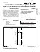
t
F2
t
F1
t
PHL
t
PLH
t
R1
t
R2
1.5V
3.0V
0V
0V
DRIVER
INPUT
V
OUT
V
OH
V
OL
3.3V
3.0V
-3.0V
-3.3V
R
L
C
L
SIGNAL
GENERATOR
Figure 1. Slew-Rate Test Circuit and Timing Diagram