
Datasheet


Fail-Safe, High-Speed (10Mbps),
Slew-Rate-Limited RS-485/RS-422 Transceivers
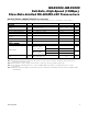
Pin Description
PIN
—95 — Noninverting Driver OutputY9
5
6
7
5
6
7
3
—
4
4
—
5
Driver Input. With DE high, a low on DI forces noninverting
output low and inverting output high. Similarly, a high on DI
forces noninverting output high and inverting output low.
DI5
Slew-Rate-Limit Selector Pin. Connect SRL to GND for 10Mbps
communication rate; connect to V
CC
for 500kbps communication
rate. Leave unconnected for 115kbps communication rate.
SRL—
GroundGND6, 7
88— — TXP—
44— 3
Driver Output Enable. Drive DE high to enable driver outputs. These
outputs are high impedance when DE is low. Drive RE high and DE
low to enter low-power shutdown mode.
DE4
2
3
HALF-
DUPLEX
MODE
1
MAX3089
2
3
FULL-
DUPLEX
MODE
1
2
—
FULL-DUPLEX
DEVICES
—
MAX3081
MAX3084
MAX3087
1
2
HALF-
DUPLEX
DEVICES
—
MAX3082
MAX3085
MAX3088
Receiver Output. When RE is low and if A - B ≥ -50mV, RO will be
high; if A - B ≤ -200mV, RO will be low.
RO2
Receiver Output Enable. Drive RE low to enable RO; RO is high
impedance when RE is high. Drive RE high and DE low to enter
low-power shutdown mode.
RE
3
FUNCTIONNAME
Half/Full-Duplex Selector Pin. Connect H/F to V
CC
for half-duplex
mode; connect to GND or leave unconnected for full-duplex mode.
H/F
—
MAX3080
MAX3083
MAX3086
Transmitter Phase. Connect TXP to GND, or leave floating for normal
transmitter phase/polarity. Connect to V
CC
to invert the transmitter
phase/polarity.
— — — — 9 Y Noninverting Receiver Input and Noninverting Driver Output*
10 6 — 10 — Z Inverting Driver Output
— — — — 10 Z Inverting Receiver Input and Inverting Driver Output*
11 7 — 11 — B Inverting Receiver Input
— — — — 11 B Receiver Input Resistors*
— — 7 — — B Inverting Receiver Input and Inverting Driver Output
PIN
MAX3080–MAX3089
10
Maxim Integrated