
Datasheet


Fail-Safe, High-Speed (10Mbps),
Slew-Rate-Limited RS-485/RS-422 Transceivers
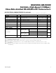
ABSOLUTE MAXIMUM RATINGS
DC ELECTRICAL CHARACTERISTICS
(V
CC
= +5V ±5%, T
A
= T
MIN
to T
MAX
, unless otherwise noted. Typical values are at V
CC
= +5V and T
A
= +25°C.) (Note 1)
Stresses beyond those listed under “Absolute Maximum Ratings” may cause permanent damage to the device. These are stress ratings only, and functional
operation of the device at these or any other conditions beyond those indicated in the operational sections of the specifications is not implied. Exposure to
absolute maximum rating conditions for extended periods may affect device reliability.
Supply Voltage (V
CC
) ............................................................+7V
Control Input Voltage (
RE, DE)...................-0.3V to (V
CC
+ 0.3V)
Special Input Voltage
(H/F, SRL, TXP, RXP)..................................-0.3V to (V
CC
+ 0.3V)
Driver Input Voltage (DI).............................-0.3V to (V
CC
+ 0.3V)
Driver Output Voltage (A, B, Y, Z)........................................±13V
Receiver Input Voltage (A, B) ..............................................±13V
Receiver Input Voltage, Full Duplex (A, B) ..........................±25V
Receiver Output Voltage (RO)....................-0.3V to (V
CC
+ 0.3V)
Continuous Power Dissipation
8-Pin Plastic DIP (derate 9.09mW/°C above +70°C) ...727mW
8-Pin SO (derate 5.88mW/°C above +70°C)................471mW
14-Pin Plastic DIP (derate 10.0mW/°C above +70°C) ....800mW
14-Pin SO (derate 8.33mW/°C above +70°C)..............667mW
Operating Temperature Ranges
MAX308_C_ _ .....................................................0°C to +70°C
MAX308_E_ _...................................................-40°C to +85°C
Storage Temperature Range .............................-65°C to +150°C
Lead Temperature (soldering, 10s) .................................+300°C
Figure 5, R = 50Ω (RS-422)
DE = GND,
V
CC
= GND or 5.25V
DE = GND,
V
CC
= GND or 5.25V
H/F, TXP, RXP, internal pulldown
DE, DI, RE
SRL = V
CC
SRL
MAX3080–MAX3085, and MAX3089 with
SRL = V
CC
or unconnected
DE, DI, RE, H/F, TXP, RXP
Figure 5, R = 50Ω or R = 27Ω
Figure 5, R = 50Ω or R = 27Ω
Figure 5, R = 50Ω or R = 27Ω
SRL (Note 3)
DE, DI, RE, H/F, TXP, RXP
SRL
CONDITIONS
µA
125
I
O
Output Leakage (Y and Z)
Full Duplex
µA
125
I
IN4
Input Current (A and B)
Full Duplex
µA
75
I
IN3
SRL Input Current
V0.8V
IL2
Input Low Voltage
V0.4V
CC
0.6V
CC
V
IM2
Input Middle Voltage
VV
CC
- 0.8V
IH2
Input High Voltage
V
2.0
V
OD2
Differential Driver Output
10 40I
IN2
µA
±2I
IN1
SRL Input Current
mV100V
HYS
DI Input Hysteresis
V0.8V
IL1
Input Low Voltage
V0.2∆V
OD
Change in Magnitude of
Differential Output Voltage
(Note 2)
V3V
OC
Driver Common-Mode Output
Voltage
V0.2∆V
OC
Change In Magnitude of
Common-Mode Voltage (Note 2)
V2.0V
IH1
Input High Voltage
UNITSMIN TYP MAXSYMBOLPARAMETER
Figure 5, R = 27Ω (RS-485) 1.5
SRL = GND (Note 3) -75
V
IN
= 12V
V
IN
= 12V
V
IN
= -7V -100
-75V
IN
= -7V
Figure 5 V5V
OD1
Differential Driver Output
(no load)
mAV
OD1
Driver Short-Circuit Output
Current (Note 4)
DRIVER
-7V ≤ V
OUT
≤ V
CC
-250
0V ≤ V
OUT
≤ 12V
0V ≤ V
OUT
≤ V
CC
±25
250
MAX3080–MAX3089
2
Maxim Integrated