
Datasheet


MAX3040–MAX3045
±10kV ESD-Protected, Quad 5V RS-485/RS-422
Transmitters
4 _______________________________________________________________________________________
Note 1: All currents into the device are positive; all currents out of the device are negative. All voltages are referenced to device
ground unless otherwise noted.
Note 2: ∆V
OD
and ∆V
OC
are the changes in V
OD
and V
OC
, respectively, when the transmitter input changes state.
Note 3: This input current level is for the hot-swap enable (EN_, EN, EN) inputs and is present until the first transition only. After the
first transition the input reverts to a standard high-impedance CMOS input with input current I
IN
. For the first 20µs the input
current may be as high as 1mA. During this period the input is disabled.
Note 4: Maximum current level applies to peak current just prior to foldback-current limiting. Minimum current level applies during
current limiting.
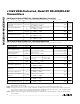
SWITCHING CHARACTERISTICS—MAX3041/MAX3044 (continued)
(V
CC
= +5V ±5%, T
A
= T
MIN
to T
MAX
, unless otherwise noted. Typical values are at V
CC
= +5V and T
A
= +25°C.)
SWITCHING CHARACTERISTICS—MAX3042B/MAX3045B
(V
CC
= +5V ±5%, T
A
= T
MIN
to T
MAX
, unless otherwise noted. Typical values are at V
CC
= +5V and T
A
= +25°C.)
PARAMETER
SYMBOL
CONDITIONS
MIN
TYP
MAX
UNITS
Maximum Data Rate f
MAX
20
Mbps
t
PLH
23 40
Driver Propagation Delay
t
PHL
Figures 2 and 3,
R
DIFF
= 54Ω, C
DIFF
= 50pF
23 40
ns
t
F
17
Driver Differential Output
Rise-Time/Fall-Time
t
R
Figures 2 and 3,
R
DIFF
= 54Ω, C
DIFF
= 50pF
17
ns
t
DSKEW
Different chips ±8
Skew Driver to Driver
t
SSKEW
Same chip
Figures 2 and 3,
R
DIFF
= 54Ω,
C
DIFF
= 50pF
±8
ns
Differential Driver Output Skew
| t
PLH
- t
PHL
|
t
SKEW
Figures 2 and 3,
R
DIFF
= 54Ω, C
DIFF
= 50pF
±8ns
Driver Enable to Output High t
ZH
MAX3042B, Figures 4 and 5, S2 closed,
R
L
= 500Ω, C
L
= 100pF
300
ns
Driver Enable from Shutdown to
Output High
t
ZH(SHDN)
Figures 4 and 5, S2 closed,
R
L
= 500Ω, C
L
= 100pF
300
ns
Driver Enable to Output Low t
ZL
MAX3042B, Figures 4 and 5, S1 closed,
R
L
= 500Ω, C
L
= 100pF
300
ns
Driver Enable from Shutdown to
Output Low
t
ZL(SHDN)
Figures 4 and 5, S1 closed,
R
L
= 500Ω, C
L
= 100pF
300
ns
Driver Disable Time from Low t
LZ
Figures 4 and 5, S1 closed,
R
L
= 500Ω, C
L
= 15pF
400
ns
Driver Disable Time from High t
HZ
Figures 4 and 5, S2 closed,
R
L
= 500Ω, C
L
= 15pF
400
ns
PARAMETER
SYMBOL
CONDITIONS
MIN
TYP
MAX
UNITS
Driver Enable from Shutdown to
Output High
t
ZH(SHDN)
Figures 4 and 5, S2 closed,
R
L
= 500Ω, C
L
= 100pF
400
ns
Driver Enable to Output Low t
ZL
MAX3041, Figures 4 and 5, S1 closed,
R
L
= 500Ω, C
L
= 100pF
400
ns
Driver Enable from Shutdown to
Output Low
t
ZL(SHDN)
Figures 4 and 5, S1 closed,
R
L
= 500Ω, C
L
= 100pF
400
ns
Driver Disable Time from Low t
LZ
Figures 4 and 5, S1 closed,
R
L
= 500Ω, C
L
= 15pF
500
ns
Driver Disable Time from High t
HZ
Figures 4 and 5, S2 closed,
R
L
= 500Ω, C
L
= 15pF
500
ns