
Datasheet


MAX3030E–MAX3033E
±15kV ESD-Protected, 3.3V Quad
RS-422 Transmitters
6 _______________________________________________________________________________________
Pin Description
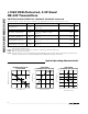
ENABLE RESPONSE TIME
MAX3030E toc13
20ns/div
ENABLE
1V/div
DIFFERENTIAL
OUTPUT
2V/div
MAX3033E EYE DIAGRAM
MAX3030E toc14
100ns/div
DO_+
1V/div
DO_-
1V/div
Typical Operating Characteristics (continued)
(V
CC
= +3.3V and T
A
= +25°C, unless otherwise noted.)
PIN
MAX3030E/
MAX3031E
MAX3032E/
MAX3033E
NAME FUNCTION
1, 7, 9, 15 1, 7, 9, 15
DI1, DI2,
DI3, DI4
Transmitter Inputs. When the corresponding transmitter is enabled, a low on DI_ forces
the noninverting output low and inverting output high. Similarly, a high on DI_ forces
noninverting output high and inverting output low.
2, 6, 10, 14 2, 6, 10, 14
DO1+, DO2+,
DO3+, DO4+
Noninverting RS-422 Outputs
3, 5, 11, 13 3, 5, 11, 13
DO1-, DO2-,
DO3-, DO4-
Inverting RS-422 Outputs
4 — EN
Transmitter Enable Input: Active HIGH. Drive EN HIGH to enable all transmitters. When
EN is HIGH, drive EN LOW to disable (three-state) all the transmitters. The transmitter
outputs are high impedance when disabled. EN is hot-swap protected (see the Hot
Swap section).
8 8 GND Ground
12 — EN
Transmitter Enable Input: Active LOW. Drive EN LOW to enable all transmitters. When
EN is LOW, drive EN HIGH to disable all the transmitters. The transmitter outputs are
high impedance when disabled. EN is hot-swap protected (see the Hot Swap section).
— 4 EN1&2
Transmitter Enable Input for Channels 1 and 2. Drive EN1&2 HIGH to enable the
corresponding transmitters. Drive EN1&2 LOW to disable the corresponding
transmitters. The transmitter outputs are high impedance when disabled. EN1&2 is hot-
swap protected (see the Hot Swap section).
— 12 EN3&4
Transmitter Enable Input for Channels 3 and 4. Drive EN3&4 HIGH to enable the
corresponding transmitters. Drive EN3&4 LOW to disable the corresponding
transmitters. The transmitter outputs are high impedance when disabled. EN3&4 is hot-
swap protected (see the Hot Swap section).
16 16 V
CC
Positive Supply; +3V ≤ V
CC
≤ +3.6V. Bypass V
CC
to GND with a 0.1µF capacitor.