
Datasheet


MAX260/MAX261/MAX262
Microprocessor Programmable
Universal Active Filters
Maxim cannot assume responsibility for use of any circuitry other than circuitry entirely embodied in a Maxim product. No circuit patent licenses are
implied. Maxim reserves the right to change the circuitry and specifications without notice at any time.
26 ____________________Maxim Integrated Products, 120 San Gabriel Drive, Sunnyvale, CA 94086 408-737-7600
© 2002 Maxim Integrated Products Printed USA is a registered trademark of Maxim Integrated Products.
Ordering Information (continued)
PART TEMP RANGE PACKAGE A C C U R A C Y
MAX261ACNG 0°C to +70°C Plastic DIP 1%
MAX261BCNG 0°C to +70°C Plastic DIP 2%
MAX261AENG -40°C to +85°C Plastic DIP 1%
MAX261BENG -40°C to +85°C Plastic DIP 2%
MAX261ACWG 0°C to +70°C Wide SO 1%
MAX261BCWG 0°C to +70°C Wide SO 2%
MAX261AMRG -55°C to +125°C CERDIP 1%
MAX261BMRG -55°C to +125°C CERDIP 2%
MAX262ACNG 0°C to +70°C Plastic DIP 1%
MAX262BCNG 0°C to +70°C Plastic DIP 2%
MAX262AENG -40°C to +85°C Plastic DIP 1%
MAX2G2BENG -40°C to +85°C Plastic DIP 2%
MAX262ACWG 0°C to +70°C Wide SO 1%
MAX262BCWG 0°C to +70°C Wide SO 2%
MAX262AMRG -55°C to +125°C CERDIP 1%
MAX262BMRG -55°C to +125°C CERDIP 2%
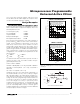
*All devices—24-pin packages 0.3in-wide packages
V
+
A1
0.199in
(5.055mm)
A2
CLK
A
CLK
B
D0
CLK OUT
N.C.(OP IN)
V
-
A0
WR
HP
B
(N.C.)
N.C.(HP
A
)
HP
A
(OP OUT)
N.C.(HP
B
)
BP
A
LP
A
IN
B
LP
B
BP
B
0.128in
3.251mm
IN
A
D1
OSC OUT
GND
A3
NOTE: LABELS IN PARENTHESES ( ) ARE FOR MAX261/MAX262 ONLY
Chip Topography