
Datasheet


Input Logic Threshold Low
MAX220–MAX249
+5V-Powered, Multichannel RS-232
Drivers/Receivers
8 _______________________________________________________________________________________
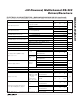
ABSOLUTE MAXIMUM RATINGS—MAX225/MAX244–MAX249
ELECTRICAL CHARACTERISTICS—MAX225/MAX244–MAX249
(MAX225, V
CC
= 5.0V ±5%; MAX244–MAX249, V
CC
= +5.0V ±10%, external capacitors C1–C4 = 1µF; T
A
= T
MIN
to T
MAX
; unless oth-
erwise noted.)
Stresses beyond those listed under “Absolute Maximum Ratings” may cause permanent damage to the device. These are stress ratings only, and functional
operation of the device at these or any other conditions beyond those indicated in the operational sections of the specifications is not implied. Exposure to
absolute maximum rating conditions for extended periods may affect device reliability.
Supply Voltage (V
CC
) ...............................................-0.3V to +6V
Input Voltages
T
IN
‚ ENA, ENB, ENR, ENT, ENRA,
ENRB, ENTA, ENTB..................................-0.3V to (V
CC
+ 0.3V)
R
IN
.....................................................................................±25V
T
OUT
(Note 5).....................................................................±15V
R
OUT
........................................................-0.3V to (V
CC
+ 0.3V)
Short Circuit (one output at a time)
T
OUT
to GND ............................................................Continuous
R
OUT
to GND............................................................Continuous
Continuous Power Dissipation (T
A
= +70°C)
28-Pin Wide SO (derate 12.50mW/°C above +70°C) .............1W
40-Pin Plastic DIP (derate 11.11mW/°C above +70°C) ...611mW
44-Pin PLCC (derate 13.33mW/°C above +70°C) ...........1.07W
Operating Temperature Ranges
MAX225C_ _, MAX24_C_ _ ..................................0°C to +70°C
MAX225E_ _, MAX24_E_ _ ...............................-40°C to +85°C
Storage Temperature Range .............................-65°C to +160°C
Lead Temperature (soldering,10s) (Note 6) ....................+300°C
V
CC
= 0V,
V
OUT
= ±15V
µATables 1a–1d
±0.01 ±25
Normal operation
Shutdown
Tables 1a–1d, normal operation
All transmitter outputs loaded with 3kΩ to GND
ENA, ENB, ENT, ENTA, ENTB =
V
CC,
V
OUT
= ±15V
VRS-232 Input Hysteresis
RS-232 Input Threshold Low V
V±5 ±7.5Output Voltage Swing
Output Leakage Current (Shutdown)
±0.01 ±25
Ω300 10MV
CC
= V+ = V- = 0V, V
OUT
= ±2V (Note 7)Transmitter Output Resistance
µA
PARAMETER
±0.05 ±0.10
MIN TYP MAX UNITS
Normal operation, outputs disabled,
Tables 1a–1d, 0V ≤ V
OUT
≤ V
CC
, ENR_ = V
CC
TTL/CMOS Output Leakage Current
10 30Shrinking V
OUT
= V
CC
mA
-2 -10Sourcing V
OUT
= GND
V3.5 V
CC
- 0.2I
OUT
= -1.0mATTL/CMOS Output Voltage High
V0.2 0.4I
OUT
= 3.2mATTL/CMOS Output Voltage Low
kΩ357
0.2 0.5 1.0V
CC
= 5V
1.4 0.8 V
TTL/CMOS Output Short-Circuit Current
V1.8 2.4
0.8 1.3V
CC
= 5V
RS-232 Input Resistance
V±25RS-232 Input Voltage Operating Range
mA±7 ±30V
OUT
= 0VOutput Short-Circuit Current
kbps120 64Data Rate
CONDITIONS
V
CC
= 5V
µA
±0.01 ±1
Logic Pullup/lnput Current
10 50
Tables 1a–1d
RS-232 Input Threshold High
V2 1.4Input Logic Threshold High
RS-232 TRANSMITTERS
RS-232 RECEIVERS
Note 5: Input voltage measured with transmitter output in a high-impedance state, shutdown, or V
CC
= 0V.
Note 6: Maximum reflow temperature for the MAX225/MAX245/MAX246/MAX247 is +225°C.