
Datasheet


Maxim Integrated | 13www.maximintegrated.com
MAX202E–MAX213E,
MAX232E/MAX241E
±15kV ESD-Protected,
5V RS-232 Transceivers
outputs. Therefore, after PC board assembly, the
Machine Model is less relevant to I/O ports.
Applications Information
Capacitor Selection
The capacitor type used for C1–C4 is not critical for
proper operation. The MAX202E, MAX206–MAX208E,
MAX211E, and MAX213E require 0.1µF capacitors,
and the MAX232E and MAX241E require 1µF capaci-
tors, although in all cases capacitors up to 10µF can
be used without harm. Ceramic, aluminum-electrolytic,
or tantalum capacitors are suggested for the 1µF
capacitors, and ceramic dielectrics are suggested for
the 0.1µF capacitors. When using the minimum recom-
mended capacitor values, make sure the capacitance
value does not degrade excessively as the operating
temperature varies. If in doubt, use capacitors with a
larger (e.g., 2x) nominal value. The capacitors’ effec-
tive series resistance (ESR), which usually rises at low
temperatures, influences the amount of ripple on V+
and V-.
Use larger capacitors (up to 10µF) to reduce the output
impedance at V+ and V-. This can be useful when
“stealing” power from V+ or from V-. The MAX203E and
MAX205E have internal charge-pump capacitors.
Bypass V
CC
to ground with at least 0.1µF. In applica-
tions sensitive to power-supply noise generated by the
charge pumps, decouple V
CC
to ground with a capaci-
tor the same size as (or larger than) the charge-pump
capacitors (C1–C4).
V+ and V- as Power Supplies
A small amount of power can be drawn from V+ and V-,
although this will reduce both driver output swing and
noise margins. Increasing the value of the charge-pump
capacitors (up to 10µF) helps maintain performance
when power is drawn from V+ or V-.
Driving Multiple Receivers
Each transmitter is designed to drive a single receiver.
Transmitters can be paralleled to drive multiple
receivers.
Driver Outputs when Exiting Shutdown
The driver outputs display no ringing or undesirable
transients as they come out of shutdown.
High Data Rates
These transceivers maintain the RS-232 ±5.0V mini-
mum driver output voltages at data rates of over
120kbps. For data rates above 120kbps, refer to the
Transmitter Output Voltage vs. Load Capacitance
graphs in the
Typical Operating Characteristics
.
Communication at these high rates is easier if the
capacitive loads on the transmitters are small; i.e.,
short cables are best.
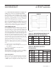
Table 2. Summary of EIA/TIA-232E, V.28 Specifications
PARAMETER CONDITIONS
EIA/TIA-232E, V.28 SPECIFICA-
TIONS
0 Level
3kΩ to 7kΩ load +5V to +15V
Data Rate 3kΩ≤R
L
≤ 7kΩ, C
L
≤ 2500pF Up to 20kbps
+3V to +15V
Instantaneous Slew Rate, Max 3kΩ≤R
L
≤ 7kΩ, C
L
≤ 2500pF 30V/µs
Driver Output Short-Circuit Current, Max 100mA
Transition Rate on Driver Output
V.28 1ms or 3% of the period
Driver Output Resistance -2V < V
OUT
< +2V 300Ω
EIA/TIA-232E 4% of the period
Driver Output Level, Max No load ±25V
Driver Output Voltage
3kΩ to 7kΩ load -5V to -15V
0 Level
1 Level
1 Level
Receiver Input Level ±25V
Receiver Input Voltage
-3V to -15V