
Datasheet


+5V, RS-232 Transceivers
with 0.1µF External Capacitors
Detailed Description
The MAX200–MAX209/MAX211/MAX213 consist of
three sections: charge-pump voltage converters, drivers
(transmitters), and receivers. Each section is described
in detail.
+5V to
±
10V Dual Charge-Pump
Voltage Converter
The +5V to Q10V conversion is performed by two
charge-pump voltage converters (Figure 4). The first
uses capacitor C1 to double +5V to +10V, storing +10V
on the V+ output filter capacitor, C3. The second charge-
pump voltage converter uses capacitor C2 to invert +10V
to -10V, storing -10V on the V- output filter capacitor, C4.
The MAX201 and MAX209 include only the V+ to V-
charge pump, and are intended for applications that
have a V
CC
= +5V supply and a V+ supply in the +9V to
+13.2V range.
In shutdown mode, V+ is internally connected to V
CC
by
a 1kI pulldown resistor and V- is internally connected to
ground by a 1kI pullup resistor.
RS-232 Drivers
When V
CC
= +5V, the typical driver output-voltage swing
is Q8V when loaded with a nominal 5kI RS-232 receiver.
The output swing is guaranteed to meet the EIA/TIA-232E
and V.28 specifications, which call for Q5V minimum out-
put levels under worst-case conditions. These include
a minimum 3kI load, V
CC
= +4.5V, and the maximum
operating temperature. The open-circuit output-voltage
swing ranges from (V+ - 0.6V) to V-.
Input thresholds are both CMOS and TTL compatible.
The inputs of unused drivers can be left unconnected
since 400kI pullup resistors to V
CC
are included on-
chip. Since all drivers invert, the pullup resistors force
the outputs of unused drivers low. The input pullup resis-
tors typically source 15µA; therefore, the driver inputs
should be driven high or open circuited to minimize
power-supply current in shutdown mode.
When in low-power shutdown mode, the driver outputs
are turned off and their leakage current is less than 1mA,
even if the transmitter output is backdriven between 0V
and (V
CC
+ 6V). Below -0.5V, the transmitter output is
diode clamped to ground with a 1kI series impedance.
The transmitter output is also zener clamped to approxi-
mately (V
CC
+ 6V), with a 1kI series impedance.
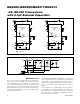
Figure 1. Shutdown Current Test Circuit
Figure 2. Receiver Output Enable and Disable Timing
I
SHDN
+5.5V
+5.5V
+5.5V (0)
+5.5V
0V OR +5.5V
DRIVE
0.1FF
0.1FF
0.1FF
0.1FF
C1+
C1-
C2+
C2-
400kI
3kI
5kI
GND
V
CC
V+
V-
T
IN
+5.5V
T1 T0 T5
R1 T0 R5
T
OUT
R
IN
0.1FF
SHDN
R
OUT
(SHDN)
EN (EN)
MAX200
MAX205
MAX206
MAX211
MAX213
NOTE 1: ( ) ARE FOR MAX213.
NOTE 2: CAPACITORS CAN BE POLARIZED OR UNPOLARIZED.
+3.5V
RECEIVER
OUTPUT
C
L
= 150pF
+0.8V
V
OH
- 0.1V
+ 2.5V
V
OH
V
OL
R
L
= 1kI
V
OL
+ 0.1V
OUTPUT ENABLE TIME
RECEIVER
OUTPUTS
+3V
0V
EN
INPUT
OUTPUT ENABLE TIME
+3V
0V
EN
INPUT
NOTE: POLARITY OF EN IS REVERSED FOR THE MAX213.
MAX200–MAX209/MAX211/MAX213
Maxim Integrated
5