
Datasheet


MAX19707
10-Bit, 45Msps, Ultra-Low-Power
Analog Front-End
32 ______________________________________________________________________________________
0
2
1
4
3
7
6
5
000 010001 011 100 101 110
AT STEP
011 (0.5 LSB)
AT STEP
001 (0.25 LSB)
111
DIGITAL INPUT CODE
ANALOG OUTPUT VALUE
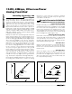
Figure 13a. Integral Nonlinearity
0
2
1
4
3
6
5
000 010001 011 100 101
DIFFERENTIAL LINEARITY
ERROR (-0.25 LSB)
DIFFERENTIAL
LINEARITY ERROR (+0.25 LSB)
1 LSB
1 LSB
DIGITAL INPUT CODE
ANALOG OUTPUT VALUE
Figure 13b. Differential Nonlinearity
Grounding, Bypassing, and
Board Layout
The MAX19707 requires high-speed board layout
design techniques. Refer to the MAX19707 EV kit data
sheet for a board layout reference. Place all bypass
capacitors as close to the device as possible, prefer-
ably on the same side of the board as the device, using
surface-mount devices for minimum inductance.
Bypass V
DD
to GND with a 0.1µF ceramic capacitor in
parallel with a 2.2µF capacitor. Bypass OV
DD
to OGND
with a 0.1µF ceramic capacitor in parallel with a 2.2µF
capacitor. Bypass REFP, REFN, and COM each to
GND with a 0.33µF ceramic capacitor. Bypass REFIN
to GND with a 0.1µF capacitor.
Multilayer boards with separated ground and power
planes yield the highest level of signal integrity. Use a
split ground plane arranged to match the physical loca-
tion of the analog ground (GND) and the digital output-
driver ground (OGND) on the device package.
Connect the MAX19707 exposed backside paddle to
GND plane. Join the two ground planes at a single
point so the noisy digital ground currents do not inter-
fere with the analog ground plane. The ideal location
for this connection can be determined experimentally
at a point along the gap between the two ground
planes. Make this connection with a low-value, surface-
mount resistor (1Ω to 5Ω), a ferrite bead, or a direct
short. Alternatively, all ground pins could share the
same ground plane, if the ground plane is sufficiently
isolated from any noisy digital system’s ground plane
(e.g., downstream output buffer or DSP ground plane).
Route high-speed digital signal traces away from sensi-
tive analog traces. Make sure to isolate the analog
input lines to each respective converter to minimize
channel-to-channel crosstalk. Keep all signal lines
short and free of 90° turns.
Dynamic Parameter Definitions
ADC and DAC Static Parameter Definitions
Integral Nonlinearity (INL)
Integral nonlinearity is the deviation of the values on an
actual transfer function from a straight line. This straight
line can be either a best-straight-line fit or a line drawn
between the end points of the transfer function, once
offset and gain errors have been nullified. The static lin-
earity parameters for the device are measured using
the best-straight-line fit (DAC Figure 13a).
Differential Nonlinearity (DNL)
Differential nonlinearity is the difference between an
actual step width and the ideal value of 1 LSB. A DNL
error specification of less than 1 LSB guarantees no
missing codes (ADC) and a monotonic transfer function
(ADC and DAC) (DAC Figure 13b).
ADC Offset Error
Ideally, the midscale transition occurs at 0.5 LSB above
midscale. The offset error is the amount of deviation
between the measured transition point and the ideal
transition point.
DAC Offset Error
Offset error (Figure 13a) is the difference between the
ideal and actual offset point. The offset point is the out-
put value when the digital input is midscale. This error
affects all codes by the same amount and usually can
be compensated by trimming.