
Datasheet


MOSFET Gate Drivers
The DH and DL drivers are designed to drive logic-level
N-channel MOSFETs to optimize system cost and effi-
ciency. MOSFETs with R
DSON
rated at V
GS
4.5V are
recommended. An adaptive dead-time circuit monitors
the DL output and prevents the high-side MOSFET from
turning on until DL is fully off. There must be a low-resis-
tance, low-inductance path from the DL driver to the
MOSFET gate for the adaptive dead-time circuit to work
properly. Otherwise, the internal sense circuitry could
interpret the MOSFET gate as “off” while there is actually
still charge left on the gate. Use very short, wide traces
measuring no more than 20 squares (50mils to 100mils
wide if the MOSFET is 1in from the IC).
Undervoltage Lockout and Soft-Start
There are two undervoltage lockout (UVLO) circuits on
the MAX1960/MAX1961/MAX1962. The first UVLO cir-
cuit monitors V
CC
, which must be above 2.15V (typ) in
order for the charge pump to operate. The second
UVLO circuit monitors the output of the charge pump.
The charge-pump output, V
DD
, must be above 4.2V
(typ) in order for the PWM converter to operate. Both
UVLO circuits inhibit switching and force DL high and DH
low when either V
CC
or V
DD
are below their threshold.
When the monitored voltages are above their thresh-
olds, an internal soft-start timer ramps up the error-
amplifier reference voltage. The ramp occurs in eighty
10mV steps. Full output voltage is reached 1.28ms after
activation with a 1MHz operating frequency.
MAX1960/MAX1961/MAX1962
2.35V to 5.5V, 0.5% Accurate, 1MHz PWM
Step-Down Controllers with Voltage Margining
______________________________________________________________________________________ 11
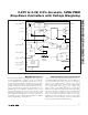
S
R
Q
Q
CURRENT
SENSE
OSC
UVLO
SOFT-START
DAC
CHARGE
PUMP
OSC
V
DD
REF
ILIM
(MAX1960/MAX1961)
FSET/SYNC
CLKOUT
COMP
FB
(MAX1960/MAX1962)
OUT
(MAX1961/MAX1962)
FEEDBACK
SELECT
VSEL
(MAX1961/MAX1962)
C+
C-
V
DD
V
CC
REF
AV
DD
PGND
GND
DL
LX
DH
BST
SHUTDOWN
AND VOLTAGE
MARGINING
CTL1
(MAX1960/MAX1961)
CTL2
(MAX1960/MAX1961)
EN
(MAX1962)
PGND
LX
CS
(MAX1962)
OSC
OUT
MAX1960/
MAX1961/
MAX1962
COMP
ERROR
AMP
Figure 1. Functional Diagram